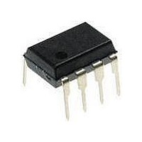
PIC12F1840-I/P Microchip Technology, PIC12F1840-I/P Datasheet - Page 91

PIC12F1840-I/P
Manufacturer Part Number
PIC12F1840-I/P
Description
7 KB Flash, 256 Bytes RAM, 32 MHz Int. Osc, 6 I/0, Enhanced Mid Range Core 8 PDI
Manufacturer
Microchip Technology
Datasheet
1.PIC12F1840-IP.pdf
(382 pages)
Specifications of PIC12F1840-I/P
Processor Series
PIC12F
Core
PIC
Program Memory Type
Flash
Program Memory Size
7 KB
Data Ram Size
256 B
Interface Type
MI2C, SPI, EUSART
Number Of Timers
3
Operating Supply Voltage
1.8 V to 5.5 V
Maximum Operating Temperature
+ 85 C
Mounting Style
Through Hole
Package / Case
PDIP-8
Development Tools By Supplier
MPLAB IDE Software
Minimum Operating Temperature
- 40 C
Lead Free Status / Rohs Status
Lead free / RoHS Compliant
Available stocks
Company
Part Number
Manufacturer
Quantity
Price
Company:
Part Number:
PIC12F1840-I/P
Manufacturer:
MICROCHIP
Quantity:
200
- Current page: 91 of 382
- Download datasheet (4Mb)
9.2
The PIC12F1840 device contains an internal Low
Dropout (LDO) voltage regulator, which allows the
device I/O pins to operate at voltages up to 5.5V while
the internal device logic operates at a lower voltage.
The LDO and its associated reference circuitry must
remain active when the device is in Sleep mode. The
PIC12F1840 allows the user to optimize the operating
current in Sleep, depending on the application require-
ments.
A Low-Power Sleep mode can be selected by setting
the VREGPM bit of the VREGCON register. With this
bit set, the LDO and reference circuitry are placed in a
low-power state when the device is in Sleep.
9.2.1
In the default operating mode, the LDO and reference
circuitry remain in the normal configuration while in
Sleep. The device is able to exit Sleep mode quickly
since all circuits remain active. In Low-Power Sleep
mode, when waking up from Sleep, an extra delay time
is required for these circuits to return to the normal con-
figuration and stabilize.
The Low-Power Sleep mode is beneficial for applica-
tions that stay in Sleep mode for long periods of time.
The normal mode is beneficial for applications that
need to wake from Sleep quickly and frequently.
REGISTER 9-1:
2011 Microchip Technology Inc.
bit 7
Legend:
R = Readable bit
u = Bit is unchanged
‘1’ = Bit is set
bit 7-2
bit 1
bit 0
Note 1:
U-0
—
Low Power Sleep Mode
PIC12F1840 only.
SLEEP CURRENT VS. WAKE-UP
TIME
Unimplemented: Read as ‘0’
VREGPM: Voltage Regulator Power Mode Selection bit
1 = Low Power Sleep mode enabled in Sleep
0 = Normal Power mode enabled in Sleep
Reserved: Read as ‘1’. Maintain this bit set.
Draws lowest current in Sleep, slower wake-up
Draws higher current in Sleep, faster wake-up
U-0
—
VREGCON: VOLTAGE REGULATOR CONTROL REGISTER
W = Writable bit
x = Bit is unknown
‘0’ = Bit is cleared
U-0
—
U-0
Preliminary
—
U = Unimplemented bit, read as ‘0’
-n/n = Value at POR and BOR/Value at all other Resets
9.2.2
Some peripherals that can operate in Sleep mode will
not operate properly with the Low-Power Sleep mode
selected. The LDO will remain in the normal power
mode when those peripherals are enabled. The Low-
Power Sleep mode is intended for use with these
peripherals:
• Brown-Out Reset (BOR)
• Watchdog Timer (WDT)
• External interrupt pin/Interrupt-on-change pins
• Timer1 (with external clock source)
• Comparator
• ECCP (Capture mode)
U-0
—
Note:
PERIPHERAL USAGE IN SLEEP
The PIC12LF1840 does not have a con-
figurable
PIC12LF1840 is an unregulated device
and is always in the lowest power state
when in Sleep, with no wake-up time pen-
alty. This device has a lower maximum
V
PIC12F1840. See
cal Specifications”
DD
U-0
PIC12(L)F1840
—
and
Low-Power
I/O
VREGPM
R/W-0/0
(1)
Section 30.0 “Electri-
voltage
for more information.
DS41441B-page 91
Sleep
Reserved
than
R/W-1/1
mode.
bit 0
the
Related parts for PIC12F1840-I/P
Image
Part Number
Description
Manufacturer
Datasheet
Request
R

Part Number:
Description:
7 KB Flash, 256 Bytes RAM, 32 MHz Int. Osc, 6 I/0, Enhanced Mid Range Core, Nano
Manufacturer:
Microchip Technology
Datasheet:

Part Number:
Description:
MCU, MPU & DSP Development Tools 8 Bit PIC Develop Microcontroller
Manufacturer:
SchmartBoard
Datasheet:

Part Number:
Description:
7 KB Flash, 256 Bytes RAM, 32 MHz Int. Osc, 6 I/0, Enhanced Mid Range Core 8 DFN
Manufacturer:
Microchip Technology

Part Number:
Description:
7 KB Flash, 256 Bytes RAM, 32 MHz Int. Osc, 6 I/0, Enhanced Mid Range Core 8 SOI
Manufacturer:
Microchip Technology

Part Number:
Description:
7 KB Flash, 256 Bytes RAM, 32 MHz Int. Osc, 6 I/0, Enhanced Mid Range Core, Nano
Manufacturer:
Microchip Technology
Datasheet:

Part Number:
Description:
7 KB Flash, 256 Bytes RAM, 32 MHz Int. Osc, 6 I/0, Enhanced Mid Range Core, Nano
Manufacturer:
Microchip Technology
Datasheet:

Part Number:
Description:
7 KB Flash, 256 Bytes RAM, 32 MHz Int. Osc, 6 I/0, Enhanced Mid Range Core, Nano
Manufacturer:
Microchip Technology
Datasheet:

Part Number:
Description:
7 KB Flash, 256 Bytes RAM, 32 MHz Int. Osc, 6 I/0, Enhanced Mid Range Core, Nano
Manufacturer:
Microchip Technology

Part Number:
Description:
7 KB Flash, 256 Bytes RAM, 32 MHz Int. Osc, 6 I/0, Enhanced Mid Range Core, Nano
Manufacturer:
Microchip Technology

Part Number:
Description:
7 KB Flash, 256 Bytes RAM, 32 MHz Int. Osc, 6 I/0, Enhanced Mid Range Core, Nano
Manufacturer:
Microchip Technology
Datasheet:

Part Number:
Description:
7 KB Flash, 256 Bytes RAM, 32 MHz Int. Osc, 6 I/0, Enhanced Mid Range Core, Nano
Manufacturer:
Microchip Technology
Datasheet:

Part Number:
Description:
Manufacturer:
Microchip Technology Inc.
Datasheet:

Part Number:
Description:
Manufacturer:
Microchip Technology Inc.
Datasheet:


