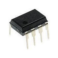
PIC12F1840-I/P Microchip Technology, PIC12F1840-I/P Datasheet - Page 109

PIC12F1840-I/P
Manufacturer Part Number
PIC12F1840-I/P
Description
7 KB Flash, 256 Bytes RAM, 32 MHz Int. Osc, 6 I/0, Enhanced Mid Range Core 8 PDI
Manufacturer
Microchip Technology
Datasheet
1.PIC12F1840-IP.pdf
(382 pages)
Specifications of PIC12F1840-I/P
Processor Series
PIC12F
Core
PIC
Program Memory Type
Flash
Program Memory Size
7 KB
Data Ram Size
256 B
Interface Type
MI2C, SPI, EUSART
Number Of Timers
3
Operating Supply Voltage
1.8 V to 5.5 V
Maximum Operating Temperature
+ 85 C
Mounting Style
Through Hole
Package / Case
PDIP-8
Development Tools By Supplier
MPLAB IDE Software
Minimum Operating Temperature
- 40 C
Lead Free Status / Rohs Status
Lead free / RoHS Compliant
Available stocks
Company
Part Number
Manufacturer
Quantity
Price
Company:
Part Number:
PIC12F1840-I/P
Manufacturer:
MICROCHIP
Quantity:
200
- Current page: 109 of 382
- Download datasheet (4Mb)
REGISTER 11-5:
2011 Microchip Technology Inc.
bit 7
Legend:
R = Readable bit
S = Bit can only be set
‘1’ = Bit is set
bit 7
bit 6
bit 5
bit 4
bit 3
bit 2
bit 1
bit 0
R/W-0/0
EEPGD
EEPGD: Flash Program/Data EEPROM Memory Select bit
1 = Accesses program space Flash memory
0 = Accesses data EEPROM memory
CFGS: Flash Program/Data EEPROM or Configuration Select bit
1 = Accesses Configuration, User ID and Device ID Registers
0 = Accesses Flash Program or data EEPROM Memory
LWLO: Load Write Latches Only bit
If CFGS = 1 (Configuration space) OR CFGS = 0 and EEPGD = 1 (program Flash):
If CFGS = 0 and EEPGD = 0: (Accessing data EEPROM)
LWLO is ignored. The next WR command initiates a write to the data EEPROM.
FREE: Program Flash Erase Enable bit
If CFGS = 1 (Configuration space) OR CFGS = 0 and EEPGD = 1 (program Flash):
If EEPGD = 0 and CFGS = 0: (Accessing data EEPROM)
FREE is ignored. The next WR command will initiate both a erase cycle and a write cycle.
WRERR: EEPROM Error Flag bit
1 = Condition indicates an improper program or erase sequence attempt or termination (bit is set
0 = The program or erase operation completed normally.
WREN: Program/Erase Enable bit
1 = Allows program/erase cycles
0 = Inhibits programming/erasing of program Flash and data EEPROM
WR: Write Control bit
1 = Initiates a program Flash or data EEPROM program/erase operation.
0 = Program/erase operation to the Flash or data EEPROM is complete and inactive.
RD: Read Control bit
1 = Initiates a program Flash or data EEPROM read. Read takes one cycle. RD is cleared in
0 = Does not initiate a program Flash or data EEPROM data read.
R/W-0/0
CFGS
1 = The next WR command does not initiate a write; only the program memory latches are
0 = The next WR command writes a value from EEDATH:EEDATL into program memory latches
1 = Performs an erase operation on the next WR command (cleared by hardware after comple-
0 = Performs a write operation on the next WR command.
automatically on any set attempt (write ‘1’) of the WR bit).
The operation is self-timed and the bit is cleared by hardware once operation is complete.
The WR bit can only be set (not cleared) in software.
hardware. The RD bit can only be set (not cleared) in software.
EECON1: EEPROM CONTROL 1 REGISTER
updated.
and initiates a write of all the data stored in the program memory latches.
tion of erase).
W = Writable bit
x = Bit is unknown
‘0’ = Bit is cleared
R/W-0/0
LWLO
R/W/HC-0/0
FREE
Preliminary
U = Unimplemented bit, read as ‘0’
-n/n = Value at POR and BOR/Value at all other Resets
HC = Bit is cleared by hardware
WRERR
R/W-x/q
R/W-0/0
WREN
PIC12(L)F1840
R/S/HC-0/0
WR
DS41441B-page 109
R/S/HC-0/0
RD
bit 0
Related parts for PIC12F1840-I/P
Image
Part Number
Description
Manufacturer
Datasheet
Request
R

Part Number:
Description:
7 KB Flash, 256 Bytes RAM, 32 MHz Int. Osc, 6 I/0, Enhanced Mid Range Core, Nano
Manufacturer:
Microchip Technology
Datasheet:

Part Number:
Description:
MCU, MPU & DSP Development Tools 8 Bit PIC Develop Microcontroller
Manufacturer:
SchmartBoard
Datasheet:

Part Number:
Description:
7 KB Flash, 256 Bytes RAM, 32 MHz Int. Osc, 6 I/0, Enhanced Mid Range Core 8 DFN
Manufacturer:
Microchip Technology

Part Number:
Description:
7 KB Flash, 256 Bytes RAM, 32 MHz Int. Osc, 6 I/0, Enhanced Mid Range Core 8 SOI
Manufacturer:
Microchip Technology

Part Number:
Description:
7 KB Flash, 256 Bytes RAM, 32 MHz Int. Osc, 6 I/0, Enhanced Mid Range Core, Nano
Manufacturer:
Microchip Technology
Datasheet:

Part Number:
Description:
7 KB Flash, 256 Bytes RAM, 32 MHz Int. Osc, 6 I/0, Enhanced Mid Range Core, Nano
Manufacturer:
Microchip Technology
Datasheet:

Part Number:
Description:
7 KB Flash, 256 Bytes RAM, 32 MHz Int. Osc, 6 I/0, Enhanced Mid Range Core, Nano
Manufacturer:
Microchip Technology
Datasheet:

Part Number:
Description:
7 KB Flash, 256 Bytes RAM, 32 MHz Int. Osc, 6 I/0, Enhanced Mid Range Core, Nano
Manufacturer:
Microchip Technology

Part Number:
Description:
7 KB Flash, 256 Bytes RAM, 32 MHz Int. Osc, 6 I/0, Enhanced Mid Range Core, Nano
Manufacturer:
Microchip Technology

Part Number:
Description:
7 KB Flash, 256 Bytes RAM, 32 MHz Int. Osc, 6 I/0, Enhanced Mid Range Core, Nano
Manufacturer:
Microchip Technology
Datasheet:

Part Number:
Description:
7 KB Flash, 256 Bytes RAM, 32 MHz Int. Osc, 6 I/0, Enhanced Mid Range Core, Nano
Manufacturer:
Microchip Technology
Datasheet:

Part Number:
Description:
Manufacturer:
Microchip Technology Inc.
Datasheet:

Part Number:
Description:
Manufacturer:
Microchip Technology Inc.
Datasheet:


