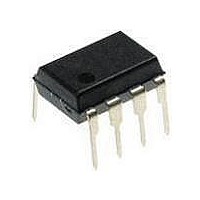
PIC12F1840-I/P Microchip Technology, PIC12F1840-I/P Datasheet - Page 273

PIC12F1840-I/P
Manufacturer Part Number
PIC12F1840-I/P
Description
7 KB Flash, 256 Bytes RAM, 32 MHz Int. Osc, 6 I/0, Enhanced Mid Range Core 8 PDI
Manufacturer
Microchip Technology
Datasheet
1.PIC12F1840-IP.pdf
(382 pages)
Specifications of PIC12F1840-I/P
Processor Series
PIC12F
Core
PIC
Program Memory Type
Flash
Program Memory Size
7 KB
Data Ram Size
256 B
Interface Type
MI2C, SPI, EUSART
Number Of Timers
3
Operating Supply Voltage
1.8 V to 5.5 V
Maximum Operating Temperature
+ 85 C
Mounting Style
Through Hole
Package / Case
PDIP-8
Development Tools By Supplier
MPLAB IDE Software
Minimum Operating Temperature
- 40 C
Lead Free Status / Rohs Status
Lead free / RoHS Compliant
Available stocks
Company
Part Number
Manufacturer
Quantity
Price
Company:
Part Number:
PIC12F1840-I/P
Manufacturer:
MICROCHIP
Quantity:
200
- Current page: 273 of 382
- Download datasheet (4Mb)
26.1.2.4
Each character in the receive FIFO buffer has a
corresponding framing error Status bit. A framing error
indicates that a Stop bit was not seen at the expected
time. The framing error status is accessed via the
FERR bit of the RCSTA register. The FERR bit
represents the status of the top unread character in the
receive FIFO. Therefore, the FERR bit must be read
before reading the RCREG.
The FERR bit is read-only and only applies to the top
unread character in the receive FIFO. A framing error
(FERR = 1) does not preclude reception of additional
characters. It is not necessary to clear the FERR bit.
Reading the next character from the FIFO buffer will
advance the FIFO to the next character and the next
corresponding framing error.
The FERR bit can be forced clear by clearing the SPEN
bit of the RCSTA register which resets the EUSART.
Clearing the CREN bit of the RCSTA register does not
affect the FERR bit. A framing error by itself does not
generate an interrupt.
26.1.2.5
The receive FIFO buffer can hold two characters. An
overrun error will be generated if a third character, in its
entirety, is received before the FIFO is accessed. When
this happens the OERR bit of the RCSTA register is set.
The characters already in the FIFO buffer can be read
but no additional characters will be received until the
error is cleared. The error must be cleared by either
clearing the CREN bit of the RCSTA register or by
resetting the EUSART by clearing the SPEN bit of the
RCSTA register.
26.1.2.6
The EUSART supports 9-bit character reception. When
the RX9 bit of the RCSTA register is set the EUSART
will shift 9 bits into the RSR for each character
received. The RX9D bit of the RCSTA register is the
ninth and Most Significant data bit of the top unread
character in the receive FIFO. When reading 9-bit data
from the receive FIFO buffer, the RX9D data bit must
be read before reading the 8 Least Significant bits from
the RCREG.
2011 Microchip Technology Inc.
Note:
If all receive characters in the receive
FIFO have framing errors, repeated reads
of the RCREG will not clear the FERR bit.
Receive Framing Error
Receive Overrun Error
Receiving 9-bit Characters
Preliminary
26.1.2.7
A special Address Detection mode is available for use
when multiple receivers share the same transmission
line, such as in RS-485 systems. Address detection is
enabled by setting the ADDEN bit of the RCSTA
register.
Address detection requires 9-bit character reception.
When address detection is enabled, only characters
with the ninth data bit set will be transferred to the
receive FIFO buffer, thereby setting the RCIF interrupt
bit. All other characters will be ignored.
Upon receiving an address character, user software
determines if the address matches its own. Upon
address match, user software must disable address
detection by clearing the ADDEN bit before the next
Stop bit occurs. When user software detects the end of
the message, determined by the message protocol
used, software places the receiver back into the
Address Detection mode by setting the ADDEN bit.
Address Detection
PIC12(L)F1840
DS41441B-page 273
Related parts for PIC12F1840-I/P
Image
Part Number
Description
Manufacturer
Datasheet
Request
R

Part Number:
Description:
7 KB Flash, 256 Bytes RAM, 32 MHz Int. Osc, 6 I/0, Enhanced Mid Range Core, Nano
Manufacturer:
Microchip Technology
Datasheet:

Part Number:
Description:
MCU, MPU & DSP Development Tools 8 Bit PIC Develop Microcontroller
Manufacturer:
SchmartBoard
Datasheet:

Part Number:
Description:
7 KB Flash, 256 Bytes RAM, 32 MHz Int. Osc, 6 I/0, Enhanced Mid Range Core 8 DFN
Manufacturer:
Microchip Technology

Part Number:
Description:
7 KB Flash, 256 Bytes RAM, 32 MHz Int. Osc, 6 I/0, Enhanced Mid Range Core 8 SOI
Manufacturer:
Microchip Technology

Part Number:
Description:
7 KB Flash, 256 Bytes RAM, 32 MHz Int. Osc, 6 I/0, Enhanced Mid Range Core, Nano
Manufacturer:
Microchip Technology
Datasheet:

Part Number:
Description:
7 KB Flash, 256 Bytes RAM, 32 MHz Int. Osc, 6 I/0, Enhanced Mid Range Core, Nano
Manufacturer:
Microchip Technology
Datasheet:

Part Number:
Description:
7 KB Flash, 256 Bytes RAM, 32 MHz Int. Osc, 6 I/0, Enhanced Mid Range Core, Nano
Manufacturer:
Microchip Technology
Datasheet:

Part Number:
Description:
7 KB Flash, 256 Bytes RAM, 32 MHz Int. Osc, 6 I/0, Enhanced Mid Range Core, Nano
Manufacturer:
Microchip Technology

Part Number:
Description:
7 KB Flash, 256 Bytes RAM, 32 MHz Int. Osc, 6 I/0, Enhanced Mid Range Core, Nano
Manufacturer:
Microchip Technology

Part Number:
Description:
7 KB Flash, 256 Bytes RAM, 32 MHz Int. Osc, 6 I/0, Enhanced Mid Range Core, Nano
Manufacturer:
Microchip Technology
Datasheet:

Part Number:
Description:
7 KB Flash, 256 Bytes RAM, 32 MHz Int. Osc, 6 I/0, Enhanced Mid Range Core, Nano
Manufacturer:
Microchip Technology
Datasheet:

Part Number:
Description:
Manufacturer:
Microchip Technology Inc.
Datasheet:

Part Number:
Description:
Manufacturer:
Microchip Technology Inc.
Datasheet:


