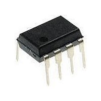
PIC12F1840-I/P Microchip Technology, PIC12F1840-I/P Datasheet - Page 141

PIC12F1840-I/P
Manufacturer Part Number
PIC12F1840-I/P
Description
7 KB Flash, 256 Bytes RAM, 32 MHz Int. Osc, 6 I/0, Enhanced Mid Range Core 8 PDI
Manufacturer
Microchip Technology
Datasheet
1.PIC12F1840-IP.pdf
(382 pages)
Specifications of PIC12F1840-I/P
Processor Series
PIC12F
Core
PIC
Program Memory Type
Flash
Program Memory Size
7 KB
Data Ram Size
256 B
Interface Type
MI2C, SPI, EUSART
Number Of Timers
3
Operating Supply Voltage
1.8 V to 5.5 V
Maximum Operating Temperature
+ 85 C
Mounting Style
Through Hole
Package / Case
PDIP-8
Development Tools By Supplier
MPLAB IDE Software
Minimum Operating Temperature
- 40 C
Lead Free Status / Rohs Status
Lead free / RoHS Compliant
Available stocks
Company
Part Number
Manufacturer
Quantity
Price
Company:
Part Number:
PIC12F1840-I/P
Manufacturer:
MICROCHIP
Quantity:
200
- Current page: 141 of 382
- Download datasheet (4Mb)
17.0
The Digital-to-Analog Converter supplies a variable
voltage reference, ratiometric with the input source,
with 32 selectable output levels.
The input of the DAC can be connected to:
• External V
• V
• FVR (Fixed Voltage Reference)
The output of the DAC can be configured to supply a
reference voltage to the following:
• Comparator positive input
• ADC input channel
• DACOUT pin
• Capacitive Sensing (CPS) module
The Digital-to-Analog Converter (DAC) can be enabled
by setting the DACEN bit of the DACCON0 register.
EQUATION 17-1:
17.2
The DAC output value is derived using a resistor ladder
with each end of the ladder tied to a positive and
negative voltage reference input source. If the voltage
of either input source fluctuates, a similar fluctuation will
result in the DAC output value.
The value of the individual resistors within the ladder
can
Specifications”.
2011 Microchip Technology Inc.
IF DACEN = 1
IF DACEN = 0 & DACLPS = 1 & DACR[4:0] = 11111
IF DACEN = 0 & DACLPS = 0 & DACR[4:0] = 00000
V
V
V
DD
V
V
SOURCE
SOURCE
OUT
OUT
OUT
supply voltage
be
DIGITAL-TO-ANALOG
CONVERTER (DAC) MODULE
Ratiometric Output Level
=
=
=
+ = V
- = V
REF
found
V
V
V
SOURCE
SOURCE
SOURCE
SS
pins
DD
, V
in
REF
+
DAC OUTPUT VOLTAGE
–
+ V
–
, or FVR BUFFER 2
Section 30.0
SOURCE
-
DACR 4:0
-----------------------------
“Electrical
2
5
Preliminary
+
V
SOURCE
17.1
The DAC has 32 voltage level ranges. The 32 levels
are set with the DACR<4:0> bits of the DACCON1
register.
The DAC output voltage is determined by the following
equations:
-
17.3
The DAC can be output to the DACOUT pin by setting
the DACOE bit of the DACCON0 register to ‘1’.
Selecting the DAC reference voltage for output on the
DACOUT pin automatically overrides the digital output
buffer and digital input threshold detector functions of
that pin. Reading the DACOUT pin when it has been
configured for DAC reference voltage output will
always return a ‘0’.
Due to the limited current drive capability, a buffer must
be used on the DAC voltage reference output for
external connections to DACOUT.
an example buffering technique.
Output Voltage Selection
DAC Voltage Reference Output
PIC12(L)F1840
Figure 17-2
DS41441B-page 141
shows
Related parts for PIC12F1840-I/P
Image
Part Number
Description
Manufacturer
Datasheet
Request
R

Part Number:
Description:
7 KB Flash, 256 Bytes RAM, 32 MHz Int. Osc, 6 I/0, Enhanced Mid Range Core, Nano
Manufacturer:
Microchip Technology
Datasheet:

Part Number:
Description:
MCU, MPU & DSP Development Tools 8 Bit PIC Develop Microcontroller
Manufacturer:
SchmartBoard
Datasheet:

Part Number:
Description:
7 KB Flash, 256 Bytes RAM, 32 MHz Int. Osc, 6 I/0, Enhanced Mid Range Core 8 DFN
Manufacturer:
Microchip Technology

Part Number:
Description:
7 KB Flash, 256 Bytes RAM, 32 MHz Int. Osc, 6 I/0, Enhanced Mid Range Core 8 SOI
Manufacturer:
Microchip Technology

Part Number:
Description:
7 KB Flash, 256 Bytes RAM, 32 MHz Int. Osc, 6 I/0, Enhanced Mid Range Core, Nano
Manufacturer:
Microchip Technology
Datasheet:

Part Number:
Description:
7 KB Flash, 256 Bytes RAM, 32 MHz Int. Osc, 6 I/0, Enhanced Mid Range Core, Nano
Manufacturer:
Microchip Technology
Datasheet:

Part Number:
Description:
7 KB Flash, 256 Bytes RAM, 32 MHz Int. Osc, 6 I/0, Enhanced Mid Range Core, Nano
Manufacturer:
Microchip Technology
Datasheet:

Part Number:
Description:
7 KB Flash, 256 Bytes RAM, 32 MHz Int. Osc, 6 I/0, Enhanced Mid Range Core, Nano
Manufacturer:
Microchip Technology

Part Number:
Description:
7 KB Flash, 256 Bytes RAM, 32 MHz Int. Osc, 6 I/0, Enhanced Mid Range Core, Nano
Manufacturer:
Microchip Technology

Part Number:
Description:
7 KB Flash, 256 Bytes RAM, 32 MHz Int. Osc, 6 I/0, Enhanced Mid Range Core, Nano
Manufacturer:
Microchip Technology
Datasheet:

Part Number:
Description:
7 KB Flash, 256 Bytes RAM, 32 MHz Int. Osc, 6 I/0, Enhanced Mid Range Core, Nano
Manufacturer:
Microchip Technology
Datasheet:

Part Number:
Description:
Manufacturer:
Microchip Technology Inc.
Datasheet:

Part Number:
Description:
Manufacturer:
Microchip Technology Inc.
Datasheet:


