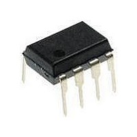
PIC12F1840-I/P Microchip Technology, PIC12F1840-I/P Datasheet - Page 176

PIC12F1840-I/P
Manufacturer Part Number
PIC12F1840-I/P
Description
7 KB Flash, 256 Bytes RAM, 32 MHz Int. Osc, 6 I/0, Enhanced Mid Range Core 8 PDI
Manufacturer
Microchip Technology
Datasheet
1.PIC12F1840-IP.pdf
(382 pages)
Specifications of PIC12F1840-I/P
Processor Series
PIC12F
Core
PIC
Program Memory Type
Flash
Program Memory Size
7 KB
Data Ram Size
256 B
Interface Type
MI2C, SPI, EUSART
Number Of Timers
3
Operating Supply Voltage
1.8 V to 5.5 V
Maximum Operating Temperature
+ 85 C
Mounting Style
Through Hole
Package / Case
PDIP-8
Development Tools By Supplier
MPLAB IDE Software
Minimum Operating Temperature
- 40 C
Lead Free Status / Rohs Status
Lead free / RoHS Compliant
Available stocks
Company
Part Number
Manufacturer
Quantity
Price
Company:
Part Number:
PIC12F1840-I/P
Manufacturer:
MICROCHIP
Quantity:
200
- Current page: 176 of 382
- Download datasheet (4Mb)
PIC12(L)F1840
22.1
The clock input to the Timer2 modules is the system
instruction clock (F
TMR2 increments from 00h on each clock edge.
A 4-bit counter/prescaler on the clock input allows direct
input, divide-by-4 and divide-by-16 prescale options.
These options are selected by the prescaler control bits,
T2CKPS<1:0> of the T2CON register. The value of
TMR2 is compared to that of the Period register, PR2, on
each clock cycle. When the two values match, the
comparator generates a match signal as the timer
output. This signal also resets the value of TMR2 to 00h
on
counter/postscaler
Interrupt”).
The TMR2 and PR2 registers are both directly readable
and writable. The TMR2 register is cleared on any
device Reset, whereas the PR2 register initializes to
FFh. Both the prescaler and postscaler counters are
cleared on the following events:
• a write to the TMR2 register
• a write to the T2CON register
• Power-on Reset (POR)
• Brown-out Reset (BOR)
• MCLR Reset
• Watchdog Timer (WDT) Reset
• Stack Overflow Reset
• Stack Underflow Reset
• RESET Instruction
22.2
Timer2 can also generate an optional device interrupt.
The Timer2 output signal (TMR2-to-PR2 match)
provides the input for the 4-bit counter/postscaler. This
counter generates the TMR2 match interrupt flag which
is latched in TMR2IF of the PIR1 register. The interrupt
is enabled by setting the TMR2 Match Interrupt Enable
bit, TMR2IE of the PIE1 register.
A range of 16 postscale options (from 1:1 through 1:16
inclusive) can be selected with the postscaler control
bits, T2OUTPS<3:0>, of the T2CON register.
DS41441B-page 176
Note:
the
Timer2 Operation
Timer2 Interrupt
next
TMR2 is not cleared when T2CON is
written.
cycle
OSC
(see
/4).
and
Section 22.2
drives
the
“Timer2
output
Preliminary
22.3
The unscaled output of TMR2 is available primarily to
the CCP1 module, where it is used as a time base for
operations in PWM mode.
Timer2 can be optionally used as the shift clock source
for the MSSP1 module operating in SPI mode.
Additional information is provided in Section 25.1
“Master SSP (MSSP1) Module Overview”
22.4
Timer2 cannot be operated while the processor is in
Sleep mode. The contents of the TMR2 and PR2
registers will remain unchanged while the processor is
in Sleep mode.
Timer2 Output
Timer2 Operation During Sleep
2011 Microchip Technology Inc.
Related parts for PIC12F1840-I/P
Image
Part Number
Description
Manufacturer
Datasheet
Request
R

Part Number:
Description:
7 KB Flash, 256 Bytes RAM, 32 MHz Int. Osc, 6 I/0, Enhanced Mid Range Core, Nano
Manufacturer:
Microchip Technology
Datasheet:

Part Number:
Description:
MCU, MPU & DSP Development Tools 8 Bit PIC Develop Microcontroller
Manufacturer:
SchmartBoard
Datasheet:

Part Number:
Description:
7 KB Flash, 256 Bytes RAM, 32 MHz Int. Osc, 6 I/0, Enhanced Mid Range Core 8 DFN
Manufacturer:
Microchip Technology

Part Number:
Description:
7 KB Flash, 256 Bytes RAM, 32 MHz Int. Osc, 6 I/0, Enhanced Mid Range Core 8 SOI
Manufacturer:
Microchip Technology

Part Number:
Description:
7 KB Flash, 256 Bytes RAM, 32 MHz Int. Osc, 6 I/0, Enhanced Mid Range Core, Nano
Manufacturer:
Microchip Technology
Datasheet:

Part Number:
Description:
7 KB Flash, 256 Bytes RAM, 32 MHz Int. Osc, 6 I/0, Enhanced Mid Range Core, Nano
Manufacturer:
Microchip Technology
Datasheet:

Part Number:
Description:
7 KB Flash, 256 Bytes RAM, 32 MHz Int. Osc, 6 I/0, Enhanced Mid Range Core, Nano
Manufacturer:
Microchip Technology
Datasheet:

Part Number:
Description:
7 KB Flash, 256 Bytes RAM, 32 MHz Int. Osc, 6 I/0, Enhanced Mid Range Core, Nano
Manufacturer:
Microchip Technology

Part Number:
Description:
7 KB Flash, 256 Bytes RAM, 32 MHz Int. Osc, 6 I/0, Enhanced Mid Range Core, Nano
Manufacturer:
Microchip Technology

Part Number:
Description:
7 KB Flash, 256 Bytes RAM, 32 MHz Int. Osc, 6 I/0, Enhanced Mid Range Core, Nano
Manufacturer:
Microchip Technology
Datasheet:

Part Number:
Description:
7 KB Flash, 256 Bytes RAM, 32 MHz Int. Osc, 6 I/0, Enhanced Mid Range Core, Nano
Manufacturer:
Microchip Technology
Datasheet:

Part Number:
Description:
Manufacturer:
Microchip Technology Inc.
Datasheet:

Part Number:
Description:
Manufacturer:
Microchip Technology Inc.
Datasheet:


