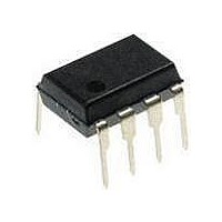
PIC12F1840-I/P Microchip Technology, PIC12F1840-I/P Datasheet - Page 89

PIC12F1840-I/P
Manufacturer Part Number
PIC12F1840-I/P
Description
7 KB Flash, 256 Bytes RAM, 32 MHz Int. Osc, 6 I/0, Enhanced Mid Range Core 8 PDI
Manufacturer
Microchip Technology
Datasheet
1.PIC12F1840-IP.pdf
(382 pages)
Specifications of PIC12F1840-I/P
Processor Series
PIC12F
Core
PIC
Program Memory Type
Flash
Program Memory Size
7 KB
Data Ram Size
256 B
Interface Type
MI2C, SPI, EUSART
Number Of Timers
3
Operating Supply Voltage
1.8 V to 5.5 V
Maximum Operating Temperature
+ 85 C
Mounting Style
Through Hole
Package / Case
PDIP-8
Development Tools By Supplier
MPLAB IDE Software
Minimum Operating Temperature
- 40 C
Lead Free Status / Rohs Status
Lead free / RoHS Compliant
Available stocks
Company
Part Number
Manufacturer
Quantity
Price
Company:
Part Number:
PIC12F1840-I/P
Manufacturer:
MICROCHIP
Quantity:
200
- Current page: 89 of 382
- Download datasheet (4Mb)
9.0
The Power-Down mode is entered by executing a
SLEEP instruction.
Upon entering Sleep mode, the following conditions
exist:
1.
2.
3.
4.
5.
6.
7.
8.
9.
10. Resets other than WDT are not affected by
Refer to individual chapters for more details on
peripheral operation during Sleep.
To minimize current consumption, the following condi-
tions should be considered:
• I/O pins should not be floating
• External circuitry sinking current from I/O pins
• Internal circuitry sourcing current from I/O pins
• Current draw from pins with internal weak pull-ups
• Modules using 31 kHz LFINTOSC
• Modules using Timer1 oscillator
I/O pins that are high-impedance inputs should be
pulled to V
currents caused by floating inputs.
Examples of internal circuitry that might be sourcing
current include modules such as the DAC and FVR
modules.
Converter (DAC) Module”
Voltage Reference (FVR)”
these modules.
2011 Microchip Technology Inc.
WDT will be cleared but keeps running, if
enabled for operation during Sleep.
PD bit of the STATUS register is cleared.
TO bit of the STATUS register is set.
CPU clock is disabled.
31 kHz LFINTOSC is unaffected and peripherals
that operate from it may continue operation in
Sleep.
Timer1 oscillator is unaffected and peripherals
that operate from it may continue operation in
Sleep.
ADC is unaffected, if the dedicated FRC clock is
selected.
Capacitive Sensing oscillator is unaffected.
I/O ports maintain the status they had before
SLEEP was executed (driving high, low or high-
impedance).
Sleep mode.
POWER-DOWN MODE (SLEEP)
DD
See
or V
Section 17.0
SS
externally to avoid switching
and
for more information on
Section 14.0 “Fixed
“Digital-to-Analog
Preliminary
9.1
The device can wake-up from Sleep through one of the
following events:
1.
2.
3.
4.
5.
6.
The first three events will cause a device Reset. The
last three events are considered a continuation of pro-
gram execution. To determine whether a device Reset
or wake-up event occurred, refer to
“Determining the Cause of a
When the SLEEP instruction is being executed, the next
instruction (PC + 1) is prefetched. For the device to
wake-up through an interrupt event, the corresponding
interrupt enable bit must be enabled. Wake-up will
occur regardless of the state of the GIE bit. If the GIE
bit is disabled, the device continues execution at the
instruction after the SLEEP instruction. If the GIE bit is
enabled, the device executes the instruction after the
SLEEP instruction, the device will call the Interrupt Ser-
vice Routine. In cases where the execution of the
instruction following SLEEP is not desirable, the user
should have a NOP after the SLEEP instruction.
The WDT is cleared when the device wakes up from
Sleep, regardless of the source of wake-up.
External Reset input on MCLR pin, if enabled
BOR Reset, if enabled
POR Reset
Watchdog Timer, if enabled
Any external interrupt
Interrupts by peripherals capable of running dur-
ing Sleep (see individual peripheral for more
information)
Wake-up from Sleep
PIC12(L)F1840
Reset”.
DS41441B-page 89
Section 7.10
Related parts for PIC12F1840-I/P
Image
Part Number
Description
Manufacturer
Datasheet
Request
R

Part Number:
Description:
7 KB Flash, 256 Bytes RAM, 32 MHz Int. Osc, 6 I/0, Enhanced Mid Range Core, Nano
Manufacturer:
Microchip Technology
Datasheet:

Part Number:
Description:
MCU, MPU & DSP Development Tools 8 Bit PIC Develop Microcontroller
Manufacturer:
SchmartBoard
Datasheet:

Part Number:
Description:
7 KB Flash, 256 Bytes RAM, 32 MHz Int. Osc, 6 I/0, Enhanced Mid Range Core 8 DFN
Manufacturer:
Microchip Technology

Part Number:
Description:
7 KB Flash, 256 Bytes RAM, 32 MHz Int. Osc, 6 I/0, Enhanced Mid Range Core 8 SOI
Manufacturer:
Microchip Technology

Part Number:
Description:
7 KB Flash, 256 Bytes RAM, 32 MHz Int. Osc, 6 I/0, Enhanced Mid Range Core, Nano
Manufacturer:
Microchip Technology
Datasheet:

Part Number:
Description:
7 KB Flash, 256 Bytes RAM, 32 MHz Int. Osc, 6 I/0, Enhanced Mid Range Core, Nano
Manufacturer:
Microchip Technology
Datasheet:

Part Number:
Description:
7 KB Flash, 256 Bytes RAM, 32 MHz Int. Osc, 6 I/0, Enhanced Mid Range Core, Nano
Manufacturer:
Microchip Technology
Datasheet:

Part Number:
Description:
7 KB Flash, 256 Bytes RAM, 32 MHz Int. Osc, 6 I/0, Enhanced Mid Range Core, Nano
Manufacturer:
Microchip Technology

Part Number:
Description:
7 KB Flash, 256 Bytes RAM, 32 MHz Int. Osc, 6 I/0, Enhanced Mid Range Core, Nano
Manufacturer:
Microchip Technology

Part Number:
Description:
7 KB Flash, 256 Bytes RAM, 32 MHz Int. Osc, 6 I/0, Enhanced Mid Range Core, Nano
Manufacturer:
Microchip Technology
Datasheet:

Part Number:
Description:
7 KB Flash, 256 Bytes RAM, 32 MHz Int. Osc, 6 I/0, Enhanced Mid Range Core, Nano
Manufacturer:
Microchip Technology
Datasheet:

Part Number:
Description:
Manufacturer:
Microchip Technology Inc.
Datasheet:

Part Number:
Description:
Manufacturer:
Microchip Technology Inc.
Datasheet:


