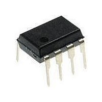
PIC12F1840-I/P Microchip Technology, PIC12F1840-I/P Datasheet - Page 249

PIC12F1840-I/P
Manufacturer Part Number
PIC12F1840-I/P
Description
7 KB Flash, 256 Bytes RAM, 32 MHz Int. Osc, 6 I/0, Enhanced Mid Range Core 8 PDI
Manufacturer
Microchip Technology
Datasheet
1.PIC12F1840-IP.pdf
(382 pages)
Specifications of PIC12F1840-I/P
Processor Series
PIC12F
Core
PIC
Program Memory Type
Flash
Program Memory Size
7 KB
Data Ram Size
256 B
Interface Type
MI2C, SPI, EUSART
Number Of Timers
3
Operating Supply Voltage
1.8 V to 5.5 V
Maximum Operating Temperature
+ 85 C
Mounting Style
Through Hole
Package / Case
PDIP-8
Development Tools By Supplier
MPLAB IDE Software
Minimum Operating Temperature
- 40 C
Lead Free Status / Rohs Status
Lead free / RoHS Compliant
Available stocks
Company
Part Number
Manufacturer
Quantity
Price
Company:
Part Number:
PIC12F1840-I/P
Manufacturer:
MICROCHIP
Quantity:
200
- Current page: 249 of 382
- Download datasheet (4Mb)
25.6.7
Master mode reception is enabled by programming the
Receive Enable bit, RCEN bit of the SSP1CON2
register.
The Baud Rate Generator begins counting and on each
rollover,
(high-to-low/low-to-high) and data is shifted into the
SSP1SR. After the falling edge of the eighth clock, the
receive enable flag is automatically cleared, the con-
tents of the SSP1SR are loaded into the SSP1BUF, the
BF flag bit is set, the SSP1IF flag bit is set and the Baud
Rate Generator is suspended from counting, holding
SCL low. The MSSP1 is now in Idle state awaiting the
next command. When the buffer is read by the CPU,
the BF flag bit is automatically cleared. The user can
then send an Acknowledge bit at the end of reception
by setting the Acknowledge Sequence Enable, ACKEN
bit of the SSP1CON2 register.
25.6.7.1
In receive operation, the BF bit is set when an address
or data byte is loaded into SSP1BUF from SSP1SR. It
is cleared when the SSP1BUF register is read.
25.6.7.2
In receive operation, the SSP1OV bit is set when 8 bits
are received into the SSP1SR and the BF flag bit is
already set from a previous reception.
25.6.7.3
If the user writes the SSP1BUF when a receive is
already in progress (i.e., SSP1SR is still shifting in a
data byte), the WCOL bit is set and the contents of the
buffer are unchanged (the write does not occur).
2011 Microchip Technology Inc.
Note:
the
I
The MSSP1 module must be in an Idle
state before the RCEN bit is set or the
RCEN bit will be disregarded.
2
C MASTER MODE RECEPTION
BF Status Flag
SSP1OV Status Flag
WCOL Status Flag
state
of
the
SCL
pin
changes
Preliminary
25.6.7.4
1.
2.
3.
4.
5.
6.
7.
8.
9.
10. Master clears SSP1IF and reads the received
11. Master sets ACK value sent to slave in ACKDT
12. Masters ACK is clocked out to the Slave and
13. User clears SSP1IF.
14. Steps 8-13 are repeated for each received byte
15. Master sends a not ACK or Stop to end
The user generates a Start condition by setting
the SEN bit of the SSP1CON2 register.
SSP1IF is set by hardware on completion of the
Start.
SSP1IF is cleared by software.
User writes SSP1BUF with the slave address to
transmit and the R/W bit set.
Address is shifted out the SDA pin until all 8 bits
are transmitted. Transmission begins as soon
as SSP1BUF is written to.
The MSSP1 module shifts in the ACK bit from
the slave device and writes its value into the
ACKSTAT bit of the SSP1CON2 register.
The MSSP1 module generates an interrupt at
the end of the ninth clock cycle by setting the
SSP1IF bit.
User sets the RCEN bit of the SSP1CON2 regis-
ter and the Master clocks in a byte from the slave.
After the 8th falling edge of SCL, SSP1IF and
BF are set.
byte from SSP1UF, clears BF.
bit of the SSP1CON2 register and initiates the
ACK by setting the ACKEN bit.
SSP1IF is set.
from the slave.
communication.
Typical Receive Sequence:
PIC12(L)F1840
DS41441B-page 249
Related parts for PIC12F1840-I/P
Image
Part Number
Description
Manufacturer
Datasheet
Request
R

Part Number:
Description:
7 KB Flash, 256 Bytes RAM, 32 MHz Int. Osc, 6 I/0, Enhanced Mid Range Core, Nano
Manufacturer:
Microchip Technology
Datasheet:

Part Number:
Description:
MCU, MPU & DSP Development Tools 8 Bit PIC Develop Microcontroller
Manufacturer:
SchmartBoard
Datasheet:

Part Number:
Description:
7 KB Flash, 256 Bytes RAM, 32 MHz Int. Osc, 6 I/0, Enhanced Mid Range Core 8 DFN
Manufacturer:
Microchip Technology

Part Number:
Description:
7 KB Flash, 256 Bytes RAM, 32 MHz Int. Osc, 6 I/0, Enhanced Mid Range Core 8 SOI
Manufacturer:
Microchip Technology

Part Number:
Description:
7 KB Flash, 256 Bytes RAM, 32 MHz Int. Osc, 6 I/0, Enhanced Mid Range Core, Nano
Manufacturer:
Microchip Technology
Datasheet:

Part Number:
Description:
7 KB Flash, 256 Bytes RAM, 32 MHz Int. Osc, 6 I/0, Enhanced Mid Range Core, Nano
Manufacturer:
Microchip Technology
Datasheet:

Part Number:
Description:
7 KB Flash, 256 Bytes RAM, 32 MHz Int. Osc, 6 I/0, Enhanced Mid Range Core, Nano
Manufacturer:
Microchip Technology
Datasheet:

Part Number:
Description:
7 KB Flash, 256 Bytes RAM, 32 MHz Int. Osc, 6 I/0, Enhanced Mid Range Core, Nano
Manufacturer:
Microchip Technology

Part Number:
Description:
7 KB Flash, 256 Bytes RAM, 32 MHz Int. Osc, 6 I/0, Enhanced Mid Range Core, Nano
Manufacturer:
Microchip Technology

Part Number:
Description:
7 KB Flash, 256 Bytes RAM, 32 MHz Int. Osc, 6 I/0, Enhanced Mid Range Core, Nano
Manufacturer:
Microchip Technology
Datasheet:

Part Number:
Description:
7 KB Flash, 256 Bytes RAM, 32 MHz Int. Osc, 6 I/0, Enhanced Mid Range Core, Nano
Manufacturer:
Microchip Technology
Datasheet:

Part Number:
Description:
Manufacturer:
Microchip Technology Inc.
Datasheet:

Part Number:
Description:
Manufacturer:
Microchip Technology Inc.
Datasheet:


