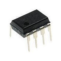
PIC12F1840-I/P Microchip Technology, PIC12F1840-I/P Datasheet - Page 132

PIC12F1840-I/P
Manufacturer Part Number
PIC12F1840-I/P
Description
7 KB Flash, 256 Bytes RAM, 32 MHz Int. Osc, 6 I/0, Enhanced Mid Range Core 8 PDI
Manufacturer
Microchip Technology
Datasheet
1.PIC12F1840-IP.pdf
(382 pages)
Specifications of PIC12F1840-I/P
Processor Series
PIC12F
Core
PIC
Program Memory Type
Flash
Program Memory Size
7 KB
Data Ram Size
256 B
Interface Type
MI2C, SPI, EUSART
Number Of Timers
3
Operating Supply Voltage
1.8 V to 5.5 V
Maximum Operating Temperature
+ 85 C
Mounting Style
Through Hole
Package / Case
PDIP-8
Development Tools By Supplier
MPLAB IDE Software
Minimum Operating Temperature
- 40 C
Lead Free Status / Rohs Status
Lead free / RoHS Compliant
Available stocks
Company
Part Number
Manufacturer
Quantity
Price
Company:
Part Number:
PIC12F1840-I/P
Manufacturer:
MICROCHIP
Quantity:
200
- Current page: 132 of 382
- Download datasheet (4Mb)
PIC12(L)F1840
16.2.6
This is an example procedure for using the ADC to
perform an Analog-to-Digital conversion:
1.
2.
3.
4.
5.
6.
7.
8.
DS41441B-page 132
Note 1: The global interrupt can be disabled if the
Configure Port:
• Disable pin output driver (Refer to the TRIS
• Configure pin as analog (Refer to the ANSEL
Configure the ADC module:
• Select ADC conversion clock
• Configure voltage reference
• Select ADC input channel
• Turn on ADC module
Configure ADC interrupt (optional):
• Clear ADC interrupt flag
• Enable ADC interrupt
• Enable peripheral interrupt
• Enable global interrupt
Wait the required acquisition time
Start conversion by setting the GO/DONE bit.
Wait for ADC conversion to complete by one of
the following:
• Polling the GO/DONE bit
• Waiting for the ADC interrupt (interrupts
Read ADC Result.
Clear the ADC interrupt flag (required if interrupt
is enabled).
register)
register)
enabled)
2: Refer to
A/D CONVERSION PROCEDURE
user is attempting to wake-up from Sleep
and resume in-line code execution.
Requirements”.
Section 16.3 “A/D Acquisition
(1)
(2)
.
Preliminary
EXAMPLE 16-1:
;This code block configures the ADC
;for polling, Vdd and Vss references, Frc
;clock and AN0 input.
;
;Conversion start & polling for completion
; are included.
;
BANKSEL
MOVLW
MOVWF
BANKSEL
BSF
BANKSEL
BSF
BANKSEL
MOVLW
MOVWF
CALL
BSF
BTFSC
GOTO
BANKSEL
MOVF
MOVWF
BANKSEL
MOVF
MOVWF
ADCON1
B’11110000’ ;Right justify, Frc
ADCON1
TRISA
TRISA,0
ANSEL
ANSEL,0
ADCON0
B’00000001’ ;Select channel AN0
ADCON0
SampleTime
ADCON0,ADGO ;Start conversion
ADCON0,ADGO ;Is conversion done?
$-1
ADRESH
ADRESH,W
RESULTHI
ADRESL
ADRESL,W
RESULTLO
A/D CONVERSION
2011 Microchip Technology Inc.
;
;clock
;Vdd and Vss Vref
;
;Set RA0 to input
;
;Set RA0 to analog
;
;Turn ADC On
;Acquisiton delay
;No, test again
;
;Read upper 2 bits
;store in GPR space
;
;Read lower 8 bits
;Store in GPR space
Related parts for PIC12F1840-I/P
Image
Part Number
Description
Manufacturer
Datasheet
Request
R

Part Number:
Description:
7 KB Flash, 256 Bytes RAM, 32 MHz Int. Osc, 6 I/0, Enhanced Mid Range Core, Nano
Manufacturer:
Microchip Technology
Datasheet:

Part Number:
Description:
MCU, MPU & DSP Development Tools 8 Bit PIC Develop Microcontroller
Manufacturer:
SchmartBoard
Datasheet:

Part Number:
Description:
7 KB Flash, 256 Bytes RAM, 32 MHz Int. Osc, 6 I/0, Enhanced Mid Range Core 8 DFN
Manufacturer:
Microchip Technology

Part Number:
Description:
7 KB Flash, 256 Bytes RAM, 32 MHz Int. Osc, 6 I/0, Enhanced Mid Range Core 8 SOI
Manufacturer:
Microchip Technology

Part Number:
Description:
7 KB Flash, 256 Bytes RAM, 32 MHz Int. Osc, 6 I/0, Enhanced Mid Range Core, Nano
Manufacturer:
Microchip Technology
Datasheet:

Part Number:
Description:
7 KB Flash, 256 Bytes RAM, 32 MHz Int. Osc, 6 I/0, Enhanced Mid Range Core, Nano
Manufacturer:
Microchip Technology
Datasheet:

Part Number:
Description:
7 KB Flash, 256 Bytes RAM, 32 MHz Int. Osc, 6 I/0, Enhanced Mid Range Core, Nano
Manufacturer:
Microchip Technology
Datasheet:

Part Number:
Description:
7 KB Flash, 256 Bytes RAM, 32 MHz Int. Osc, 6 I/0, Enhanced Mid Range Core, Nano
Manufacturer:
Microchip Technology

Part Number:
Description:
7 KB Flash, 256 Bytes RAM, 32 MHz Int. Osc, 6 I/0, Enhanced Mid Range Core, Nano
Manufacturer:
Microchip Technology

Part Number:
Description:
7 KB Flash, 256 Bytes RAM, 32 MHz Int. Osc, 6 I/0, Enhanced Mid Range Core, Nano
Manufacturer:
Microchip Technology
Datasheet:

Part Number:
Description:
7 KB Flash, 256 Bytes RAM, 32 MHz Int. Osc, 6 I/0, Enhanced Mid Range Core, Nano
Manufacturer:
Microchip Technology
Datasheet:

Part Number:
Description:
Manufacturer:
Microchip Technology Inc.
Datasheet:

Part Number:
Description:
Manufacturer:
Microchip Technology Inc.
Datasheet:


