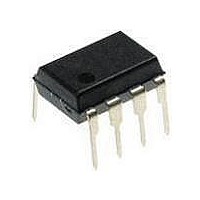
PIC12F1840-I/P Microchip Technology, PIC12F1840-I/P Datasheet - Page 155

PIC12F1840-I/P
Manufacturer Part Number
PIC12F1840-I/P
Description
7 KB Flash, 256 Bytes RAM, 32 MHz Int. Osc, 6 I/0, Enhanced Mid Range Core 8 PDI
Manufacturer
Microchip Technology
Datasheet
1.PIC12F1840-IP.pdf
(382 pages)
Specifications of PIC12F1840-I/P
Processor Series
PIC12F
Core
PIC
Program Memory Type
Flash
Program Memory Size
7 KB
Data Ram Size
256 B
Interface Type
MI2C, SPI, EUSART
Number Of Timers
3
Operating Supply Voltage
1.8 V to 5.5 V
Maximum Operating Temperature
+ 85 C
Mounting Style
Through Hole
Package / Case
PDIP-8
Development Tools By Supplier
MPLAB IDE Software
Minimum Operating Temperature
- 40 C
Lead Free Status / Rohs Status
Lead free / RoHS Compliant
Available stocks
Company
Part Number
Manufacturer
Quantity
Price
Company:
Part Number:
PIC12F1840-I/P
Manufacturer:
MICROCHIP
Quantity:
200
- Current page: 155 of 382
- Download datasheet (4Mb)
19.7
The C1NCH bit of the CM1CON1 register directs one
of two analog pins to the comparator inverting input.
19.8
The comparator output is indeterminate for a period of
time after the change of an input source or the selection
of a new reference voltage. This period is referred to as
the response time. The response time of the comparator
differs from the settling time of the voltage reference.
Therefore, both of these times must be considered when
determining the total response time to a comparator
input change. See the Comparator and Voltage Refer-
ence Specifications in Section 30.0 “Electrical Specifi-
cations” for more details.
19.9
The C1 comparator can be used as a general purpose
comparator. The output can be brought out to the
C1OUT pin. When the ECCP auto-shutdown is active
it can use the comparator signal. If auto-restart is also
enabled, the comparator can be configured as a
closed loop analog feedback to the ECCP, thereby,
creating an analog controlled PWM.
2011 Microchip Technology Inc.
Note:
Note:
Comparator Negative Input
Selection
Comparator Response Time
Interaction with ECCP Logic
To use C1IN+ and C1INx- pins as analog
input, the appropriate bits must be set in
the ANSEL register and the correspond-
ing TRIS bits must also be set to disable
the output drivers.
When the comparator module is first
initialized the output state is unknown.
Upon initialization, the user should verify
the output state of the comparator prior to
relying on the result, primarily when using
the result in connection with other
peripheral features, such as the ECCP
Auto-Shutdown mode.
Preliminary
19.10 Analog Input Connection
A simplified circuit for an analog input is shown in
Figure
connection with a digital input, they have reverse
biased ESD protection diodes to V
analog input, therefore, must be between V
If the input voltage deviates from this range by more
than 0.6V in either direction, one of the diodes is for-
ward biased and a latch-up may occur.
A maximum source impedance of 10 k is recommended
for the analog sources. Also, any external component
connected to an analog input pin, such as a capacitor or
a Zener diode, should have very little leakage current to
minimize inaccuracies introduced.
Note 1: When reading a PORT register, all pins
19-3. Since the analog input pins share their
2: Analog levels on any pin defined as a
Considerations
configured as analog inputs will read as a
‘0’. Pins configured as digital inputs will
convert as an analog input, according to
the input specification.
digital input, may cause the input buffer to
consume more current than is specified.
PIC12(L)F1840
DS41441B-page 155
DD
and V
SS
and V
SS
. The
DD
.
Related parts for PIC12F1840-I/P
Image
Part Number
Description
Manufacturer
Datasheet
Request
R

Part Number:
Description:
7 KB Flash, 256 Bytes RAM, 32 MHz Int. Osc, 6 I/0, Enhanced Mid Range Core, Nano
Manufacturer:
Microchip Technology
Datasheet:

Part Number:
Description:
MCU, MPU & DSP Development Tools 8 Bit PIC Develop Microcontroller
Manufacturer:
SchmartBoard
Datasheet:

Part Number:
Description:
7 KB Flash, 256 Bytes RAM, 32 MHz Int. Osc, 6 I/0, Enhanced Mid Range Core 8 DFN
Manufacturer:
Microchip Technology

Part Number:
Description:
7 KB Flash, 256 Bytes RAM, 32 MHz Int. Osc, 6 I/0, Enhanced Mid Range Core 8 SOI
Manufacturer:
Microchip Technology

Part Number:
Description:
7 KB Flash, 256 Bytes RAM, 32 MHz Int. Osc, 6 I/0, Enhanced Mid Range Core, Nano
Manufacturer:
Microchip Technology
Datasheet:

Part Number:
Description:
7 KB Flash, 256 Bytes RAM, 32 MHz Int. Osc, 6 I/0, Enhanced Mid Range Core, Nano
Manufacturer:
Microchip Technology
Datasheet:

Part Number:
Description:
7 KB Flash, 256 Bytes RAM, 32 MHz Int. Osc, 6 I/0, Enhanced Mid Range Core, Nano
Manufacturer:
Microchip Technology
Datasheet:

Part Number:
Description:
7 KB Flash, 256 Bytes RAM, 32 MHz Int. Osc, 6 I/0, Enhanced Mid Range Core, Nano
Manufacturer:
Microchip Technology

Part Number:
Description:
7 KB Flash, 256 Bytes RAM, 32 MHz Int. Osc, 6 I/0, Enhanced Mid Range Core, Nano
Manufacturer:
Microchip Technology

Part Number:
Description:
7 KB Flash, 256 Bytes RAM, 32 MHz Int. Osc, 6 I/0, Enhanced Mid Range Core, Nano
Manufacturer:
Microchip Technology
Datasheet:

Part Number:
Description:
7 KB Flash, 256 Bytes RAM, 32 MHz Int. Osc, 6 I/0, Enhanced Mid Range Core, Nano
Manufacturer:
Microchip Technology
Datasheet:

Part Number:
Description:
Manufacturer:
Microchip Technology Inc.
Datasheet:

Part Number:
Description:
Manufacturer:
Microchip Technology Inc.
Datasheet:


