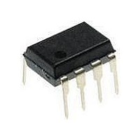
PIC12F1840-I/P Microchip Technology, PIC12F1840-I/P Datasheet - Page 198

PIC12F1840-I/P
Manufacturer Part Number
PIC12F1840-I/P
Description
7 KB Flash, 256 Bytes RAM, 32 MHz Int. Osc, 6 I/0, Enhanced Mid Range Core 8 PDI
Manufacturer
Microchip Technology
Datasheet
1.PIC12F1840-IP.pdf
(382 pages)
Specifications of PIC12F1840-I/P
Processor Series
PIC12F
Core
PIC
Program Memory Type
Flash
Program Memory Size
7 KB
Data Ram Size
256 B
Interface Type
MI2C, SPI, EUSART
Number Of Timers
3
Operating Supply Voltage
1.8 V to 5.5 V
Maximum Operating Temperature
+ 85 C
Mounting Style
Through Hole
Package / Case
PDIP-8
Development Tools By Supplier
MPLAB IDE Software
Minimum Operating Temperature
- 40 C
Lead Free Status / Rohs Status
Lead free / RoHS Compliant
Available stocks
Company
Part Number
Manufacturer
Quantity
Price
Company:
Part Number:
PIC12F1840-I/P
Manufacturer:
MICROCHIP
Quantity:
200
- Current page: 198 of 382
- Download datasheet (4Mb)
PIC12(L)F1840
24.4
The enhanced PWM mode generates a Pulse-Width
Modulation (PWM) signal on up to two different output
pins with up to 10 bits of resolution. The period, duty
cycle, and resolution are controlled by the following
registers:
• PR2 registers
• T2CON registers
• CCPR1L registers
• CCP1CON registers
The ECCP modules have the following additional PWM
registers which control Auto-shutdown, Auto-restart,
Dead-band Delay and PWM Steering modes:
• CCP1AS registers
• PSTR1CON registers
• PWM1CON registers
The enhanced PWM module can generate the following
three PWM Output modes:
• Single PWM
• Half-Bridge PWM
• Single PWM with PWM Steering Mode
To select an Enhanced PWM Output mode, the P1M bits
of the CCP1CON register must be configured
appropriately.
FIGURE 24-5:
DS41441B-page 198
Note 1:
CCPR1H (Slave)
Duty Cycle Registers
Comparator
PWM (Enhanced Mode)
CCPR1L
PR2
TMR2
Comparator
The 8-bit timer TMR1 register is concatenated with the 2-bit internal Q clock, or 2 bits of the prescaler to create the 10-bit time
base.
(1)
EXAMPLE SIMPLIFIED BLOCK DIAGRAM OF THE ENHANCED PWM MODE
Clear Timer,
toggle PWM pin and
latch duty cycle
DC1B<1:0>
R
S
P1M<1:0>
Q
Preliminary
PWM1CON
Controller
Output
2
CCP1/P1A
P1B
The PWM outputs are multiplexed with I/O pins and are
designated P1A and P1B. The polarity of the PWM pins
is configurable and is selected by setting the bits
CCP1M<3:0> in the CCP1CON register appropriately.
Figure 24-5
diagram of the Enhanced PWM module.
Table 24-8
Enhanced PWM modes.
4
CCP1M<3:0>
Note 1: The corresponding TRIS bit must be
2: Clearing the CCP1CON register will
3: Any pin not used in the enhanced PWM
4: To
TRISx
TRISx
shows the pin assignments for various
cleared to enable the PWM output on the
CCP1 pin.
relinquish control of the CCP1 pin.
mode is available for alternate pin
functions, if applicable.
incomplete waveform when the PWM is
first enabled, the ECCP module waits
until the start of a new PWM period
before generating a PWM signal.
shows an example of a simplified block
prevent
2011 Microchip Technology Inc.
the
CCP1/P1A
P1B
generation
of
an
Related parts for PIC12F1840-I/P
Image
Part Number
Description
Manufacturer
Datasheet
Request
R

Part Number:
Description:
7 KB Flash, 256 Bytes RAM, 32 MHz Int. Osc, 6 I/0, Enhanced Mid Range Core, Nano
Manufacturer:
Microchip Technology
Datasheet:

Part Number:
Description:
MCU, MPU & DSP Development Tools 8 Bit PIC Develop Microcontroller
Manufacturer:
SchmartBoard
Datasheet:

Part Number:
Description:
7 KB Flash, 256 Bytes RAM, 32 MHz Int. Osc, 6 I/0, Enhanced Mid Range Core 8 DFN
Manufacturer:
Microchip Technology

Part Number:
Description:
7 KB Flash, 256 Bytes RAM, 32 MHz Int. Osc, 6 I/0, Enhanced Mid Range Core 8 SOI
Manufacturer:
Microchip Technology

Part Number:
Description:
7 KB Flash, 256 Bytes RAM, 32 MHz Int. Osc, 6 I/0, Enhanced Mid Range Core, Nano
Manufacturer:
Microchip Technology
Datasheet:

Part Number:
Description:
7 KB Flash, 256 Bytes RAM, 32 MHz Int. Osc, 6 I/0, Enhanced Mid Range Core, Nano
Manufacturer:
Microchip Technology
Datasheet:

Part Number:
Description:
7 KB Flash, 256 Bytes RAM, 32 MHz Int. Osc, 6 I/0, Enhanced Mid Range Core, Nano
Manufacturer:
Microchip Technology
Datasheet:

Part Number:
Description:
7 KB Flash, 256 Bytes RAM, 32 MHz Int. Osc, 6 I/0, Enhanced Mid Range Core, Nano
Manufacturer:
Microchip Technology

Part Number:
Description:
7 KB Flash, 256 Bytes RAM, 32 MHz Int. Osc, 6 I/0, Enhanced Mid Range Core, Nano
Manufacturer:
Microchip Technology

Part Number:
Description:
7 KB Flash, 256 Bytes RAM, 32 MHz Int. Osc, 6 I/0, Enhanced Mid Range Core, Nano
Manufacturer:
Microchip Technology
Datasheet:

Part Number:
Description:
7 KB Flash, 256 Bytes RAM, 32 MHz Int. Osc, 6 I/0, Enhanced Mid Range Core, Nano
Manufacturer:
Microchip Technology
Datasheet:

Part Number:
Description:
Manufacturer:
Microchip Technology Inc.
Datasheet:

Part Number:
Description:
Manufacturer:
Microchip Technology Inc.
Datasheet:


