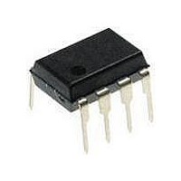
PIC12F1840-I/P Microchip Technology, PIC12F1840-I/P Datasheet - Page 294

PIC12F1840-I/P
Manufacturer Part Number
PIC12F1840-I/P
Description
7 KB Flash, 256 Bytes RAM, 32 MHz Int. Osc, 6 I/0, Enhanced Mid Range Core 8 PDI
Manufacturer
Microchip Technology
Datasheet
1.PIC12F1840-IP.pdf
(382 pages)
Specifications of PIC12F1840-I/P
Processor Series
PIC12F
Core
PIC
Program Memory Type
Flash
Program Memory Size
7 KB
Data Ram Size
256 B
Interface Type
MI2C, SPI, EUSART
Number Of Timers
3
Operating Supply Voltage
1.8 V to 5.5 V
Maximum Operating Temperature
+ 85 C
Mounting Style
Through Hole
Package / Case
PDIP-8
Development Tools By Supplier
MPLAB IDE Software
Minimum Operating Temperature
- 40 C
Lead Free Status / Rohs Status
Lead free / RoHS Compliant
Available stocks
Company
Part Number
Manufacturer
Quantity
Price
Company:
Part Number:
PIC12F1840-I/P
Manufacturer:
MICROCHIP
Quantity:
200
- Current page: 294 of 382
- Download datasheet (4Mb)
PIC12(L)F1840
26.5
The EUSART will remain active during Sleep only in the
Synchronous Slave mode. All other modes require the
system clock and therefore cannot generate the neces-
sary signals to run the Transmit or Receive Shift regis-
ters during Sleep.
Synchronous Slave mode uses an externally generated
clock to run the Transmit and Receive Shift registers.
26.5.1
To receive during Sleep, all the following conditions
must be met before entering Sleep mode:
• RCSTA and TXSTA Control registers must be
• If interrupts are desired, set the RCIE bit of the
• The RCIF interrupt flag must be cleared by read-
Upon entering Sleep mode, the device will be ready to
accept data and clocks on the RX/DT and TX/CK pins,
respectively. When the data word has been completely
clocked in by the external device, the RCIF interrupt
flag bit of the PIR1 register will be set. Thereby, waking
the processor from Sleep.
Upon waking from Sleep, the instruction following the
SLEEP instruction will be executed. If the Global Inter-
rupt Enable (GIE) bit of the INTCON register is also set,
then the Interrupt Service Routine at address 004h will
be called.
DS41441B-page 294
configured for Synchronous Slave Reception (see
Section 26.4.2.4 “Synchronous Slave
Reception
PIE1 register and the GIE and PEIE bits of the
INTCON register.
ing RCREG to unload any pending characters in
the receive buffer.
EUSART Operation During Sleep
SYNCHRONOUS RECEIVE DURING
SLEEP
Set-up:”).
Preliminary
26.5.2
To transmit during Sleep, all the following conditions
must be met before entering Sleep mode:
• RCSTA and TXSTA Control registers must be
• The TXIF interrupt flag must be cleared by writing
• If interrupts are desired, set the TXIE bit of the
• Interrupt enable bits TXIE of the PIE1 register and
Upon entering Sleep mode, the device will be ready to
accept clocks on TX/CK pin and transmit data on the
RX/DT pin. When the data word in the TSR has been
completely clocked out by the external device, the
pending byte in the TXREG will transfer to the TSR and
the TXIF flag will be set. Thereby, waking the processor
from Sleep. At this point, the TXREG is available to
accept another character for transmission, which will
clear the TXIF flag.
Upon waking from Sleep, the instruction following the
SLEEP instruction will be executed. If the Global
Interrupt Enable (GIE) bit is also set then the Interrupt
Service Routine at address 0004h will be called.
26.5.3
This module incorporates I/O pins that can be moved to
other locations with the use of the alternate pin function
register, APFCON. To determine which pins can be
moved and what their default locations are upon a
Reset, see
more information.
configured for Synchronous Slave Transmission
(see
Transmission
the output data to the TXREG, thereby filling the
TSR and transmit buffer.
PIE1 register and the PEIE bit of the INTCON reg-
ister.
PEIE of the INTCON register must set.
Section 26.4.2.2 “Synchronous Slave
Section 12.1 “Alternate Pin Function”
SYNCHRONOUS TRANSMIT
DURING SLEEP
ALTERNATE PIN LOCATIONS
Set-up:”).
2011 Microchip Technology Inc.
for
Related parts for PIC12F1840-I/P
Image
Part Number
Description
Manufacturer
Datasheet
Request
R

Part Number:
Description:
7 KB Flash, 256 Bytes RAM, 32 MHz Int. Osc, 6 I/0, Enhanced Mid Range Core, Nano
Manufacturer:
Microchip Technology
Datasheet:

Part Number:
Description:
MCU, MPU & DSP Development Tools 8 Bit PIC Develop Microcontroller
Manufacturer:
SchmartBoard
Datasheet:

Part Number:
Description:
7 KB Flash, 256 Bytes RAM, 32 MHz Int. Osc, 6 I/0, Enhanced Mid Range Core 8 DFN
Manufacturer:
Microchip Technology

Part Number:
Description:
7 KB Flash, 256 Bytes RAM, 32 MHz Int. Osc, 6 I/0, Enhanced Mid Range Core 8 SOI
Manufacturer:
Microchip Technology

Part Number:
Description:
7 KB Flash, 256 Bytes RAM, 32 MHz Int. Osc, 6 I/0, Enhanced Mid Range Core, Nano
Manufacturer:
Microchip Technology
Datasheet:

Part Number:
Description:
7 KB Flash, 256 Bytes RAM, 32 MHz Int. Osc, 6 I/0, Enhanced Mid Range Core, Nano
Manufacturer:
Microchip Technology
Datasheet:

Part Number:
Description:
7 KB Flash, 256 Bytes RAM, 32 MHz Int. Osc, 6 I/0, Enhanced Mid Range Core, Nano
Manufacturer:
Microchip Technology
Datasheet:

Part Number:
Description:
7 KB Flash, 256 Bytes RAM, 32 MHz Int. Osc, 6 I/0, Enhanced Mid Range Core, Nano
Manufacturer:
Microchip Technology

Part Number:
Description:
7 KB Flash, 256 Bytes RAM, 32 MHz Int. Osc, 6 I/0, Enhanced Mid Range Core, Nano
Manufacturer:
Microchip Technology

Part Number:
Description:
7 KB Flash, 256 Bytes RAM, 32 MHz Int. Osc, 6 I/0, Enhanced Mid Range Core, Nano
Manufacturer:
Microchip Technology
Datasheet:

Part Number:
Description:
7 KB Flash, 256 Bytes RAM, 32 MHz Int. Osc, 6 I/0, Enhanced Mid Range Core, Nano
Manufacturer:
Microchip Technology
Datasheet:

Part Number:
Description:
Manufacturer:
Microchip Technology Inc.
Datasheet:

Part Number:
Description:
Manufacturer:
Microchip Technology Inc.
Datasheet:


