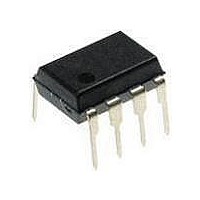
PIC12F1840-I/P Microchip Technology, PIC12F1840-I/P Datasheet - Page 259

PIC12F1840-I/P
Manufacturer Part Number
PIC12F1840-I/P
Description
7 KB Flash, 256 Bytes RAM, 32 MHz Int. Osc, 6 I/0, Enhanced Mid Range Core 8 PDI
Manufacturer
Microchip Technology
Datasheet
1.PIC12F1840-IP.pdf
(382 pages)
Specifications of PIC12F1840-I/P
Processor Series
PIC12F
Core
PIC
Program Memory Type
Flash
Program Memory Size
7 KB
Data Ram Size
256 B
Interface Type
MI2C, SPI, EUSART
Number Of Timers
3
Operating Supply Voltage
1.8 V to 5.5 V
Maximum Operating Temperature
+ 85 C
Mounting Style
Through Hole
Package / Case
PDIP-8
Development Tools By Supplier
MPLAB IDE Software
Minimum Operating Temperature
- 40 C
Lead Free Status / Rohs Status
Lead free / RoHS Compliant
Available stocks
Company
Part Number
Manufacturer
Quantity
Price
Company:
Part Number:
PIC12F1840-I/P
Manufacturer:
MICROCHIP
Quantity:
200
- Current page: 259 of 382
- Download datasheet (4Mb)
25.7
The MSSP1 module has a Baud Rate Generator avail-
able for clock generation in both I
modes. The Baud Rate Generator (BRG) reload value
is placed in the SSP1ADD register
When a write occurs to SSP1BUF, the Baud Rate Gen-
erator will automatically begin counting down.
Once the given operation is complete, the internal clock
will automatically stop counting and the clock pin will
remain in its last state.
An internal signal “Reload” in
value from SSP1ADD to be loaded into the BRG
counter. This occurs twice for each oscillation of the
FIGURE 25-40:
TABLE 25-4:
2011 Microchip Technology Inc.
Note 1:
Note: Values of 0x00, 0x01 and 0x02 are not valid
BAUD RATE GENERATOR
for SSP1ADD when used as a Baud Rate
Generator for I
limitation.
32 MHz
32 MHz
32 MHz
16 MHz
16 MHz
16 MHz
4 MHz
The I
100 kHz) in all details, but may be used with care where higher rates are required by the application.
F
OSC
2
C interface does not conform to the 400 kHz I
MSSP1 CLOCK RATE W/BRG
BAUD RATE GENERATOR BLOCK DIAGRAM
2
C. This is an implementation
SSP1M<3:0>
Figure 25-39
SCL
2
C and SPI Master
(Register
8 MHz
8 MHz
8 MHz
4 MHz
4 MHz
4 MHz
1 MHz
SSP1M<3:0>
F
triggers the
CY
Control
Reload
25-6).
SSP1CLK
Preliminary
Reload
module clock line. The logic dictating when the reload
signal is asserted depends on the mode the MSSP1 is
being operated in.
Table 25-4
instruction cycles and the BRG value loaded into
SSP1ADD.
EQUATION 25-1:
2
C specification (which applies to rates greater than
BRG Down Counter
SSP1ADD<7:0>
BRG Value
0Ch
4Fh
13h
19h
09h
27h
09h
F
CLOCK
demonstrates clock rates based on
PIC12(L)F1840
=
-------------------------------------------------
SSPxADD
F
OSC
(2 Rollovers of BRG)
/2
F
OSC
400 kHz
400 kHz
DS41441B-page 259
308 kHz
100 kHz
308 kHz
100 kHz
100 kHz
F
+
CLOCK
1
4
(1)
(1)
Related parts for PIC12F1840-I/P
Image
Part Number
Description
Manufacturer
Datasheet
Request
R

Part Number:
Description:
7 KB Flash, 256 Bytes RAM, 32 MHz Int. Osc, 6 I/0, Enhanced Mid Range Core, Nano
Manufacturer:
Microchip Technology
Datasheet:

Part Number:
Description:
MCU, MPU & DSP Development Tools 8 Bit PIC Develop Microcontroller
Manufacturer:
SchmartBoard
Datasheet:

Part Number:
Description:
7 KB Flash, 256 Bytes RAM, 32 MHz Int. Osc, 6 I/0, Enhanced Mid Range Core 8 DFN
Manufacturer:
Microchip Technology

Part Number:
Description:
7 KB Flash, 256 Bytes RAM, 32 MHz Int. Osc, 6 I/0, Enhanced Mid Range Core 8 SOI
Manufacturer:
Microchip Technology

Part Number:
Description:
7 KB Flash, 256 Bytes RAM, 32 MHz Int. Osc, 6 I/0, Enhanced Mid Range Core, Nano
Manufacturer:
Microchip Technology
Datasheet:

Part Number:
Description:
7 KB Flash, 256 Bytes RAM, 32 MHz Int. Osc, 6 I/0, Enhanced Mid Range Core, Nano
Manufacturer:
Microchip Technology
Datasheet:

Part Number:
Description:
7 KB Flash, 256 Bytes RAM, 32 MHz Int. Osc, 6 I/0, Enhanced Mid Range Core, Nano
Manufacturer:
Microchip Technology
Datasheet:

Part Number:
Description:
7 KB Flash, 256 Bytes RAM, 32 MHz Int. Osc, 6 I/0, Enhanced Mid Range Core, Nano
Manufacturer:
Microchip Technology

Part Number:
Description:
7 KB Flash, 256 Bytes RAM, 32 MHz Int. Osc, 6 I/0, Enhanced Mid Range Core, Nano
Manufacturer:
Microchip Technology

Part Number:
Description:
7 KB Flash, 256 Bytes RAM, 32 MHz Int. Osc, 6 I/0, Enhanced Mid Range Core, Nano
Manufacturer:
Microchip Technology
Datasheet:

Part Number:
Description:
7 KB Flash, 256 Bytes RAM, 32 MHz Int. Osc, 6 I/0, Enhanced Mid Range Core, Nano
Manufacturer:
Microchip Technology
Datasheet:

Part Number:
Description:
Manufacturer:
Microchip Technology Inc.
Datasheet:

Part Number:
Description:
Manufacturer:
Microchip Technology Inc.
Datasheet:


