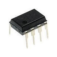
PIC12F1840-I/P Microchip Technology, PIC12F1840-I/P Datasheet - Page 209

PIC12F1840-I/P
Manufacturer Part Number
PIC12F1840-I/P
Description
7 KB Flash, 256 Bytes RAM, 32 MHz Int. Osc, 6 I/0, Enhanced Mid Range Core 8 PDI
Manufacturer
Microchip Technology
Datasheet
1.PIC12F1840-IP.pdf
(382 pages)
Specifications of PIC12F1840-I/P
Processor Series
PIC12F
Core
PIC
Program Memory Type
Flash
Program Memory Size
7 KB
Data Ram Size
256 B
Interface Type
MI2C, SPI, EUSART
Number Of Timers
3
Operating Supply Voltage
1.8 V to 5.5 V
Maximum Operating Temperature
+ 85 C
Mounting Style
Through Hole
Package / Case
PDIP-8
Development Tools By Supplier
MPLAB IDE Software
Minimum Operating Temperature
- 40 C
Lead Free Status / Rohs Status
Lead free / RoHS Compliant
Available stocks
Company
Part Number
Manufacturer
Quantity
Price
Company:
Part Number:
PIC12F1840-I/P
Manufacturer:
MICROCHIP
Quantity:
200
- Current page: 209 of 382
- Download datasheet (4Mb)
REGISTER 24-3:
REGISTER 24-4:
2011 Microchip Technology Inc.
bit 7
Legend:
R = Readable bit
u = Bit is unchanged
‘1’ = Bit is set
bit 7
bit 6-0
Note 1:
bit 7
Legend:
R = Readable bit
u = Bit is unchanged
‘1’ = Bit is set
bit 7-5
bit 4
bit 3-2
bit 1
bit 0
Note 1:
P1RSEN
R/W-0/0
U-0
—
Bit resets to ‘0’ with Two-Speed Start-up and LP, XT or HS selected as the Oscillator mode or Fail-Safe
mode is enabled.
The PWM Steering mode is available only when the CCP1CON register bits CCP1M<3:2> = 11 and
P1M<1:0> = 00.
P1RSEN: PWM Restart Enable bit
1 = Upon auto-shutdown, the CCP1ASE bit clears automatically once the shutdown event goes
0 = Upon auto-shutdown, CCP1ASE must be cleared in software to restart the PWM
P1DC<6:0>: PWM Delay Count bits
P1DC1 = Number of F
Unimplemented: Read as ‘0’
STR1SYNC: Steering Sync bit
1 = Output steering update occurs on next PWM period
0 = Output steering update occurs at the beginning of the instruction cycle boundary
Reserved: Read as ‘0’. Maintain these bits clear.
STR1B: Steering Enable bit B
1 = P1B pin has the PWM waveform with polarity control from CCP1M<1:0>
0 = P1B pin is assigned to port pin
STR1A: Steering Enable bit A
1 = P1A pin has the PWM waveform with polarity control from CCP1M<1:0>
0 = P1A pin is assigned to port pin
R/W-0/0
away; the PWM restarts automatically
U-0
—
PWM1CON: ENHANCED PWM CONTROL REGISTER
PSTR1CON: PWM STEERING CONTROL REGISTER
should transition active and the actual time it transitions active
W = Writable bit
x = Bit is unknown
‘0’ = Bit is cleared
W = Writable bit
x = Bit is unknown
‘0’ = Bit is cleared
R/W-0/0
U-0
—
OSC
/4 (4 * T
STR1SYNC
R/W-0/0
R/W-0/0
Preliminary
OSC
) cycles between the scheduled time when a PWM signal
U = Unimplemented bit, read as ‘0’
-n/n = Value at POR and BOR/Value at all other Resets
U = Unimplemented bit, read as ‘0’
-n/n = Value at POR and BOR/Value at all other Resets
P1DC<6:0>
Reserved
R/W-0/0
R/W-0/0
Reserved
R/W-0/0
R/W-0/0
PIC12(L)F1840
(1)
R/W-0/0
R/W-0/0
STR1B
DS41441B-page 209
R/W-0/0
R/W-1/1
STR1A
bit 0
bit 0
Related parts for PIC12F1840-I/P
Image
Part Number
Description
Manufacturer
Datasheet
Request
R

Part Number:
Description:
7 KB Flash, 256 Bytes RAM, 32 MHz Int. Osc, 6 I/0, Enhanced Mid Range Core, Nano
Manufacturer:
Microchip Technology
Datasheet:

Part Number:
Description:
MCU, MPU & DSP Development Tools 8 Bit PIC Develop Microcontroller
Manufacturer:
SchmartBoard
Datasheet:

Part Number:
Description:
7 KB Flash, 256 Bytes RAM, 32 MHz Int. Osc, 6 I/0, Enhanced Mid Range Core 8 DFN
Manufacturer:
Microchip Technology

Part Number:
Description:
7 KB Flash, 256 Bytes RAM, 32 MHz Int. Osc, 6 I/0, Enhanced Mid Range Core 8 SOI
Manufacturer:
Microchip Technology

Part Number:
Description:
7 KB Flash, 256 Bytes RAM, 32 MHz Int. Osc, 6 I/0, Enhanced Mid Range Core, Nano
Manufacturer:
Microchip Technology
Datasheet:

Part Number:
Description:
7 KB Flash, 256 Bytes RAM, 32 MHz Int. Osc, 6 I/0, Enhanced Mid Range Core, Nano
Manufacturer:
Microchip Technology
Datasheet:

Part Number:
Description:
7 KB Flash, 256 Bytes RAM, 32 MHz Int. Osc, 6 I/0, Enhanced Mid Range Core, Nano
Manufacturer:
Microchip Technology
Datasheet:

Part Number:
Description:
7 KB Flash, 256 Bytes RAM, 32 MHz Int. Osc, 6 I/0, Enhanced Mid Range Core, Nano
Manufacturer:
Microchip Technology

Part Number:
Description:
7 KB Flash, 256 Bytes RAM, 32 MHz Int. Osc, 6 I/0, Enhanced Mid Range Core, Nano
Manufacturer:
Microchip Technology

Part Number:
Description:
7 KB Flash, 256 Bytes RAM, 32 MHz Int. Osc, 6 I/0, Enhanced Mid Range Core, Nano
Manufacturer:
Microchip Technology
Datasheet:

Part Number:
Description:
7 KB Flash, 256 Bytes RAM, 32 MHz Int. Osc, 6 I/0, Enhanced Mid Range Core, Nano
Manufacturer:
Microchip Technology
Datasheet:

Part Number:
Description:
Manufacturer:
Microchip Technology Inc.
Datasheet:

Part Number:
Description:
Manufacturer:
Microchip Technology Inc.
Datasheet:


