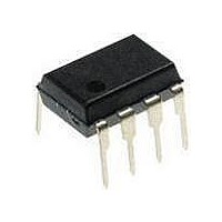
PIC12F1840-I/P Microchip Technology, PIC12F1840-I/P Datasheet - Page 270

PIC12F1840-I/P
Manufacturer Part Number
PIC12F1840-I/P
Description
7 KB Flash, 256 Bytes RAM, 32 MHz Int. Osc, 6 I/0, Enhanced Mid Range Core 8 PDI
Manufacturer
Microchip Technology
Datasheet
1.PIC12F1840-IP.pdf
(382 pages)
Specifications of PIC12F1840-I/P
Processor Series
PIC12F
Core
PIC
Program Memory Type
Flash
Program Memory Size
7 KB
Data Ram Size
256 B
Interface Type
MI2C, SPI, EUSART
Number Of Timers
3
Operating Supply Voltage
1.8 V to 5.5 V
Maximum Operating Temperature
+ 85 C
Mounting Style
Through Hole
Package / Case
PDIP-8
Development Tools By Supplier
MPLAB IDE Software
Minimum Operating Temperature
- 40 C
Lead Free Status / Rohs Status
Lead free / RoHS Compliant
Available stocks
Company
Part Number
Manufacturer
Quantity
Price
Company:
Part Number:
PIC12F1840-I/P
Manufacturer:
MICROCHIP
Quantity:
200
- Current page: 270 of 382
- Download datasheet (4Mb)
PIC12(L)F1840
26.1.1.4
The TRMT bit of the TXSTA register indicates the
status of the TSR register. This is a read-only bit. The
TRMT bit is set when the TSR register is empty and is
cleared when a character is transferred to the TSR
register from the TXREG. The TRMT bit remains clear
until all bits have been shifted out of the TSR register.
No interrupt logic is tied to this bit, so the user has to
poll this bit to determine the TSR status.
26.1.1.5
The EUSART supports 9-bit character transmissions.
When the TX9 bit of the TXSTA register is set, the
EUSART will shift 9 bits out for each character transmit-
ted. The TX9D bit of the TXSTA register is the ninth,
and Most Significant, data bit. When transmitting 9-bit
data, the TX9D data bit must be written before writing
the 8 Least Significant bits into the TXREG. All nine bits
of data will be transferred to the TSR shift register
immediately after the TXREG is written.
A special 9-bit Address mode is available for use with
multiple receivers. See
Detection”
FIGURE 26-3:
FIGURE 26-4:
DS41441B-page 270
Note:
Reg. Empty Flag)
Reg. Empty Flag)
Note:
Reg. Empty Flag)
Reg. Empty Flag)
Write to TXREG
(Transmit Buffer
Write to TXREG
(Transmit Buffer
(Transmit Shift
(Transmit Shift
BRG Output
(Shift Clock)
BRG Output
(Shift Clock)
TRMT bit
TRMT bit
TXIF bit
TXIF bit
The TSR register is not mapped in data
memory, so it is not available to the user.
for more information on the address mode.
TX/CK
TX/CK
This timing diagram shows two consecutive transmissions.
TSR Status
Transmitting 9-Bit Characters
pin
pin
ASYNCHRONOUS TRANSMISSION
ASYNCHRONOUS TRANSMISSION (BACK-TO-BACK)
1 T
Word 1
Transmit Shift Reg.
CY
Word 1
Transmit Shift Reg.
Section 26.1.2.7 “Address
Word 1
Word 1
1 T
CY
Start bit
Start bit
Word 2
1 T
CY
bit 0
bit 0
Preliminary
bit 1
Word 1
bit 1
Word 1
26.1.1.6
1.
2.
3.
4.
5.
6.
7.
Initialize the SPBRGH, SPBRGL register pair and
the BRGH and BRG16 bits to achieve the desired
baud rate (see
Rate Generator
Enable the asynchronous serial port by clearing
the SYNC bit and setting the SPEN bit.
If 9-bit transmission is desired, set the TX9 con-
trol bit. A set ninth data bit will indicate that the 8
Least Significant data bits are an address when
the receiver is set for address detection.
Enable the transmission by setting the TXEN
control bit. This will cause the TXIF interrupt bit
to be set.
If interrupts are desired, set the TXIE interrupt
enable bit of the PIE1 register. An interrupt will
occur immediately provided that the GIE and
PEIE bits of the INTCON register are also set.
If 9-bit transmission is selected, the ninth bit
should be loaded into the TX9D data bit.
Load 8-bit data into the TXREG register. This
will start the transmission.
Asynchronous Transmission Set-up:
bit 7/8
bit 7/8
Section 26.3 “EUSART Baud
(BRG)”).
Word 2
Transmit Shift Reg.
2011 Microchip Technology Inc.
Stop bit
Stop bit
Start bit
Word 2
bit 0
Related parts for PIC12F1840-I/P
Image
Part Number
Description
Manufacturer
Datasheet
Request
R

Part Number:
Description:
7 KB Flash, 256 Bytes RAM, 32 MHz Int. Osc, 6 I/0, Enhanced Mid Range Core, Nano
Manufacturer:
Microchip Technology
Datasheet:

Part Number:
Description:
MCU, MPU & DSP Development Tools 8 Bit PIC Develop Microcontroller
Manufacturer:
SchmartBoard
Datasheet:

Part Number:
Description:
7 KB Flash, 256 Bytes RAM, 32 MHz Int. Osc, 6 I/0, Enhanced Mid Range Core 8 DFN
Manufacturer:
Microchip Technology

Part Number:
Description:
7 KB Flash, 256 Bytes RAM, 32 MHz Int. Osc, 6 I/0, Enhanced Mid Range Core 8 SOI
Manufacturer:
Microchip Technology

Part Number:
Description:
7 KB Flash, 256 Bytes RAM, 32 MHz Int. Osc, 6 I/0, Enhanced Mid Range Core, Nano
Manufacturer:
Microchip Technology
Datasheet:

Part Number:
Description:
7 KB Flash, 256 Bytes RAM, 32 MHz Int. Osc, 6 I/0, Enhanced Mid Range Core, Nano
Manufacturer:
Microchip Technology
Datasheet:

Part Number:
Description:
7 KB Flash, 256 Bytes RAM, 32 MHz Int. Osc, 6 I/0, Enhanced Mid Range Core, Nano
Manufacturer:
Microchip Technology
Datasheet:

Part Number:
Description:
7 KB Flash, 256 Bytes RAM, 32 MHz Int. Osc, 6 I/0, Enhanced Mid Range Core, Nano
Manufacturer:
Microchip Technology

Part Number:
Description:
7 KB Flash, 256 Bytes RAM, 32 MHz Int. Osc, 6 I/0, Enhanced Mid Range Core, Nano
Manufacturer:
Microchip Technology

Part Number:
Description:
7 KB Flash, 256 Bytes RAM, 32 MHz Int. Osc, 6 I/0, Enhanced Mid Range Core, Nano
Manufacturer:
Microchip Technology
Datasheet:

Part Number:
Description:
7 KB Flash, 256 Bytes RAM, 32 MHz Int. Osc, 6 I/0, Enhanced Mid Range Core, Nano
Manufacturer:
Microchip Technology
Datasheet:

Part Number:
Description:
Manufacturer:
Microchip Technology Inc.
Datasheet:

Part Number:
Description:
Manufacturer:
Microchip Technology Inc.
Datasheet:


