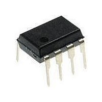
PIC12F1840-I/P Microchip Technology, PIC12F1840-I/P Datasheet - Page 343

PIC12F1840-I/P
Manufacturer Part Number
PIC12F1840-I/P
Description
7 KB Flash, 256 Bytes RAM, 32 MHz Int. Osc, 6 I/0, Enhanced Mid Range Core 8 PDI
Manufacturer
Microchip Technology
Datasheet
1.PIC12F1840-IP.pdf
(382 pages)
Specifications of PIC12F1840-I/P
Processor Series
PIC12F
Core
PIC
Program Memory Type
Flash
Program Memory Size
7 KB
Data Ram Size
256 B
Interface Type
MI2C, SPI, EUSART
Number Of Timers
3
Operating Supply Voltage
1.8 V to 5.5 V
Maximum Operating Temperature
+ 85 C
Mounting Style
Through Hole
Package / Case
PDIP-8
Development Tools By Supplier
MPLAB IDE Software
Minimum Operating Temperature
- 40 C
Lead Free Status / Rohs Status
Lead free / RoHS Compliant
Available stocks
Company
Part Number
Manufacturer
Quantity
Price
Company:
Part Number:
PIC12F1840-I/P
Manufacturer:
MICROCHIP
Quantity:
200
- Current page: 343 of 382
- Download datasheet (4Mb)
FIGURE 30-11:
TABLE 30-7:
TABLE 30-8:
2011 Microchip Technology Inc.
Standard Operating Conditions (unless otherwise stated)
Operating Temperature
CC01* TccL
CC02* TccH
CC03* TccP
Standard Operating Conditions (unless otherwise stated)
Operating temperature
AD01
AD02
AD03
AD04
AD05
AD06
AD07
AD08
Note 1: Total Absolute Error includes integral, differential, offset and gain errors.
Param
Param
No.
No.
*
†
*
†
2: The A/D conversion result never decreases with an increase in the input voltage and has no missing codes.
3: ADC V
4: When ADC is off, it will not consume any current other than leakage current. The power-down current specification
5: FVR voltage selected must be 2.048V or 4.096V.
Note:
N
E
E
E
E
V
V
Z
Sym.
Sym.
REF
AIN
AIN
R
IL
DL
OFF
GN
These parameters are characterized but not tested.
Data in “Typ” column is at 3.0V, 25°C unless otherwise stated. These parameters are for design guidance only and are not
tested.
These parameters are characterized but not tested.
Data in “Typ” column is at 3.0V, 25°C unless otherwise stated. These parameters are for design guidance only and are not
tested.
includes any such leakage from the ADC module.
Refer to
Resolution
Integral Error
Differential Error
Offset Error
Gain Error
Reference Voltage
Full-Scale Range
Recommended Impedance of
Analog Voltage Source
CCP Input High Time
CCP Input Low Time
CCP Input Period
(Capture mode)
REF
CAPTURE/COMPARE/PWM REQUIREMENTS (CCP)
PIC12(L)F1840 A/D CONVERTER (ADC) CHARACTERISTICS:
is from external V
Figure 30-5
CAPTURE/COMPARE/PWM TIMINGS (CCP)
Characteristic
-40°C T
T
A
CCP
25°C
Characteristic
(3)
A
for load conditions.
+125°C
REF
, V
With Prescaler
With Prescaler
No Prescaler
No Prescaler
DD
pin or FVR, whichever is selected as reference input.
Min.
V
1.8
—
—
—
—
—
—
SS
Preliminary
Typ†
0.5T
0.5T
—
—
—
—
—
—
—
—
3T
CC01
CY
Min.
CY
CY
20
20
N
+ 40
+ 20
+ 20
Max.
V
±1.7
±1.5
V
10
±1
±2
10
REF
DD
CC03
Typ†
Units
—
—
—
—
—
LSb V
LSb No missing codes
LSb V
LSb V
k
bit
V
V
CC02
Max.
V
V
Can go higher if external 0.01
present on input pin.
—
—
—
—
—
REF
REF
REF
REF
REF
PIC12(L)F1840
= 3.0V
= 3.0V
= 3.0V
= 3.0V
= (V
Units
ns
ns
ns
ns
ns
REF
+ minus V
N = prescale value (1, 4 or 16)
Conditions
REF
Conditions
-) (NOTE 5)
DS41441B-page 343
F capacitor is
Related parts for PIC12F1840-I/P
Image
Part Number
Description
Manufacturer
Datasheet
Request
R

Part Number:
Description:
7 KB Flash, 256 Bytes RAM, 32 MHz Int. Osc, 6 I/0, Enhanced Mid Range Core, Nano
Manufacturer:
Microchip Technology
Datasheet:

Part Number:
Description:
MCU, MPU & DSP Development Tools 8 Bit PIC Develop Microcontroller
Manufacturer:
SchmartBoard
Datasheet:

Part Number:
Description:
7 KB Flash, 256 Bytes RAM, 32 MHz Int. Osc, 6 I/0, Enhanced Mid Range Core 8 DFN
Manufacturer:
Microchip Technology

Part Number:
Description:
7 KB Flash, 256 Bytes RAM, 32 MHz Int. Osc, 6 I/0, Enhanced Mid Range Core 8 SOI
Manufacturer:
Microchip Technology

Part Number:
Description:
7 KB Flash, 256 Bytes RAM, 32 MHz Int. Osc, 6 I/0, Enhanced Mid Range Core, Nano
Manufacturer:
Microchip Technology
Datasheet:

Part Number:
Description:
7 KB Flash, 256 Bytes RAM, 32 MHz Int. Osc, 6 I/0, Enhanced Mid Range Core, Nano
Manufacturer:
Microchip Technology
Datasheet:

Part Number:
Description:
7 KB Flash, 256 Bytes RAM, 32 MHz Int. Osc, 6 I/0, Enhanced Mid Range Core, Nano
Manufacturer:
Microchip Technology
Datasheet:

Part Number:
Description:
7 KB Flash, 256 Bytes RAM, 32 MHz Int. Osc, 6 I/0, Enhanced Mid Range Core, Nano
Manufacturer:
Microchip Technology

Part Number:
Description:
7 KB Flash, 256 Bytes RAM, 32 MHz Int. Osc, 6 I/0, Enhanced Mid Range Core, Nano
Manufacturer:
Microchip Technology

Part Number:
Description:
7 KB Flash, 256 Bytes RAM, 32 MHz Int. Osc, 6 I/0, Enhanced Mid Range Core, Nano
Manufacturer:
Microchip Technology
Datasheet:

Part Number:
Description:
7 KB Flash, 256 Bytes RAM, 32 MHz Int. Osc, 6 I/0, Enhanced Mid Range Core, Nano
Manufacturer:
Microchip Technology
Datasheet:

Part Number:
Description:
Manufacturer:
Microchip Technology Inc.
Datasheet:

Part Number:
Description:
Manufacturer:
Microchip Technology Inc.
Datasheet:


