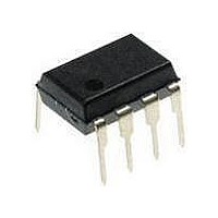
PIC12F1840-I/P Microchip Technology, PIC12F1840-I/P Datasheet - Page 44

PIC12F1840-I/P
Manufacturer Part Number
PIC12F1840-I/P
Description
7 KB Flash, 256 Bytes RAM, 32 MHz Int. Osc, 6 I/0, Enhanced Mid Range Core 8 PDI
Manufacturer
Microchip Technology
Datasheet
1.PIC12F1840-IP.pdf
(382 pages)
Specifications of PIC12F1840-I/P
Processor Series
PIC12F
Core
PIC
Program Memory Type
Flash
Program Memory Size
7 KB
Data Ram Size
256 B
Interface Type
MI2C, SPI, EUSART
Number Of Timers
3
Operating Supply Voltage
1.8 V to 5.5 V
Maximum Operating Temperature
+ 85 C
Mounting Style
Through Hole
Package / Case
PDIP-8
Development Tools By Supplier
MPLAB IDE Software
Minimum Operating Temperature
- 40 C
Lead Free Status / Rohs Status
Lead free / RoHS Compliant
Available stocks
Company
Part Number
Manufacturer
Quantity
Price
Company:
Part Number:
PIC12F1840-I/P
Manufacturer:
MICROCHIP
Quantity:
200
- Current page: 44 of 382
- Download datasheet (4Mb)
PIC12(L)F1840
REGISTER 4-2:
DS41441B-page 44
bit 13
bit 6
Legend:
R = Readable bit
u = Bit is unchanged
‘1’ = Bit is set
bit 13
bit 12
bit 11
bit 10
bit 9
bit 8
bit 7-5
bit 4
bit 3-2
bit 1-0
Note 1:
R/P-1/1
LVP
U-1
2:
—
The LVP bit cannot be programmed to ‘0’ when Programming mode is entered via LVP.
The DEBUG bit in Configuration Word is managed automatically by device development tools including debuggers and
programmers. For normal device operation, this bit should be maintained as a '1'.
LVP: Low-Voltage Programming Enable bit
1 = Low-voltage programming enabled
0 = High-voltage on MCLR must be used for programming
DEBUG: In-Circuit Debugger Mode bit
1 = In-Circuit Debugger disabled, ICSPCLK and ICSPDAT are general purpose I/O pins
0 = In-Circuit Debugger enabled, ICSPCLK and ICSPDAT are dedicated to the debugger
Unimplemented: Read as ‘1’
BORV: Brown-out Reset Voltage Selection bit
PIC12F1840:
1 = Brown-out Reset voltage set to 2.4V (typical)
0 = Brown-out Reset voltage set to 2.7V (typical)
PIC12LF1840:
1 = Brown-out Reset voltage set to 1.9V (typical)
0 = Brown-out Reset voltage set to 2.7V (typical)
STVREN: Stack Overflow/Underflow Reset Enable bit
1 = Stack Overflow or Underflow will cause a Reset
0 = Stack Overflow or Underflow will not cause a Reset
PLLEN: PLL Enable bit
1 = 4xPLL enabled
0 = 4xPLL disabled
Unimplemented: Read as ‘1’
Reserved: This location should be programmed to a ‘1’.
Unimplemented: Read as ‘1’
WRT<1:0>: Flash Memory Self-Write Protection bits
11 = Write protection off
10 = 000h to 1FFh write-protected, 200h to FFFh may be modified by EECON control
01 = 000h to 7FFh write-protected, 800h to FFFh may be modified by EECON control
00 = 000h to FFFh write-protected, no addresses may be modified by EECON control
DEBUG
R/P-1/1
CONFIGURATION WORD 2
U-1
—
(2)
W = Writable bit
‘0’ = Bit is cleared
x = Bit is unknown
Reserved
U-1
R-1
—
Preliminary
(2)
R/P-1/1
(1)
BORV
U-1
—
U = Unimplemented bit, read as ‘1’
-n/n = Value at POR and BOR/Value at all other Resets
P = Programmable bit
STVREN
R/P-1/1
U-1
—
2011 Microchip Technology Inc.
R/P-1/1
R/P-1/1
PLLEN
WRT1
R/P-1/1
WRT0
U-1
—
bit 7
bit 0
Related parts for PIC12F1840-I/P
Image
Part Number
Description
Manufacturer
Datasheet
Request
R

Part Number:
Description:
7 KB Flash, 256 Bytes RAM, 32 MHz Int. Osc, 6 I/0, Enhanced Mid Range Core, Nano
Manufacturer:
Microchip Technology
Datasheet:

Part Number:
Description:
MCU, MPU & DSP Development Tools 8 Bit PIC Develop Microcontroller
Manufacturer:
SchmartBoard
Datasheet:

Part Number:
Description:
7 KB Flash, 256 Bytes RAM, 32 MHz Int. Osc, 6 I/0, Enhanced Mid Range Core 8 DFN
Manufacturer:
Microchip Technology

Part Number:
Description:
7 KB Flash, 256 Bytes RAM, 32 MHz Int. Osc, 6 I/0, Enhanced Mid Range Core 8 SOI
Manufacturer:
Microchip Technology

Part Number:
Description:
7 KB Flash, 256 Bytes RAM, 32 MHz Int. Osc, 6 I/0, Enhanced Mid Range Core, Nano
Manufacturer:
Microchip Technology
Datasheet:

Part Number:
Description:
7 KB Flash, 256 Bytes RAM, 32 MHz Int. Osc, 6 I/0, Enhanced Mid Range Core, Nano
Manufacturer:
Microchip Technology
Datasheet:

Part Number:
Description:
7 KB Flash, 256 Bytes RAM, 32 MHz Int. Osc, 6 I/0, Enhanced Mid Range Core, Nano
Manufacturer:
Microchip Technology
Datasheet:

Part Number:
Description:
7 KB Flash, 256 Bytes RAM, 32 MHz Int. Osc, 6 I/0, Enhanced Mid Range Core, Nano
Manufacturer:
Microchip Technology

Part Number:
Description:
7 KB Flash, 256 Bytes RAM, 32 MHz Int. Osc, 6 I/0, Enhanced Mid Range Core, Nano
Manufacturer:
Microchip Technology

Part Number:
Description:
7 KB Flash, 256 Bytes RAM, 32 MHz Int. Osc, 6 I/0, Enhanced Mid Range Core, Nano
Manufacturer:
Microchip Technology
Datasheet:

Part Number:
Description:
7 KB Flash, 256 Bytes RAM, 32 MHz Int. Osc, 6 I/0, Enhanced Mid Range Core, Nano
Manufacturer:
Microchip Technology
Datasheet:

Part Number:
Description:
Manufacturer:
Microchip Technology Inc.
Datasheet:

Part Number:
Description:
Manufacturer:
Microchip Technology Inc.
Datasheet:


