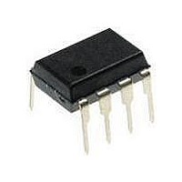
PIC12F1840-I/P Microchip Technology, PIC12F1840-I/P Datasheet - Page 129

PIC12F1840-I/P
Manufacturer Part Number
PIC12F1840-I/P
Description
7 KB Flash, 256 Bytes RAM, 32 MHz Int. Osc, 6 I/0, Enhanced Mid Range Core 8 PDI
Manufacturer
Microchip Technology
Datasheet
1.PIC12F1840-IP.pdf
(382 pages)
Specifications of PIC12F1840-I/P
Processor Series
PIC12F
Core
PIC
Program Memory Type
Flash
Program Memory Size
7 KB
Data Ram Size
256 B
Interface Type
MI2C, SPI, EUSART
Number Of Timers
3
Operating Supply Voltage
1.8 V to 5.5 V
Maximum Operating Temperature
+ 85 C
Mounting Style
Through Hole
Package / Case
PDIP-8
Development Tools By Supplier
MPLAB IDE Software
Minimum Operating Temperature
- 40 C
Lead Free Status / Rohs Status
Lead free / RoHS Compliant
Available stocks
Company
Part Number
Manufacturer
Quantity
Price
Company:
Part Number:
PIC12F1840-I/P
Manufacturer:
MICROCHIP
Quantity:
200
- Current page: 129 of 382
- Download datasheet (4Mb)
TABLE 16-1:
FIGURE 16-2:
2011 Microchip Technology Inc.
Legend:
Note 1:
Clock Source
ADC Clock Period (T
Fosc/16
Fosc/32
Fosc/64
Fosc/2
Fosc/4
Fosc/8
ADC
F
2:
3:
4:
RC
T
Set GO bit
CY
Holding capacitor is disconnected from analog input (typically 100 ns)
Shaded cells are outside of recommended range.
The F
These values violate the minimum required T
For faster conversion times, the selection of another clock source is recommended.
The ADC clock period (T
system clock F
device in Sleep mode.
- T
AD
Conversion starts
RC
ADCS<2:0>
ADC CLOCK PERIOD (T
T
AD
source has a typical T
000
100
001
101
010
110
x11
1 T
ANALOG-TO-DIGITAL CONVERSION T
AD
OSC
)
AD
b9
. However, the F
2 T
1.0-6.0 s
0.5 s
62.5ns
125 ns
AD
32 MHz
AD
b8
800 ns
1.0 s
2.0 s
3 T
) and total ADC conversion time can be minimized when the ADC clock is derived from the
(2)
(2)
(2)
AD
AD
(1,4)
b7
time of 1.6 s for V
4 T
RC
1.0-6.0 s
clock source must be used when conversions are to be performed with the
AD
AD
b6
100 ns
200 ns
400 ns
20 MHz
800 ns
5 T
1.6 s
3.2 s
) V
On the following cycle:
ADRESH:ADRESL is loaded, GO bit is cleared,
ADIF bit is set, holding capacitor is connected to analog input.
Preliminary
AD
S
AD
(2)
(2)
(2)
b5
. DEVICE OPERATING FREQUENCIES
time.
(1,4)
6 T
DD
AD
1.0-6.0 s
b4
.
Device Frequency (F
125 ns
250 ns
7 T
0.5 s
16 MHz
1.0 s
2.0 s
4.0 s
AD
b3
(2)
(2)
(2)
AD
8
(1,4)
CYCLES
T
AD
b2
1.0-6.0 s
9 T
250 ns
500 ns
8.0 s
8 MHz
1.0 s
2.0 s
4.0 s
AD
PIC12(L)F1840
b1
OSC
10
(3)
(2)
(2)
(1,4)
)
T
AD
b0
11
1.0-6.0 s
16.0 s
500 ns
8.0 s
4 MHz
1.0 s
2.0 s
4.0 s
(3)
(2)
(3)
(1,4)
DS41441B-page 129
1.0-6.0 s
16.0 s
32.0 s
64.0 s
8.0 s
1 MHz
2.0 s
4.0 s
(3)
(3)
(3)
(3)
(1,4)
Related parts for PIC12F1840-I/P
Image
Part Number
Description
Manufacturer
Datasheet
Request
R

Part Number:
Description:
7 KB Flash, 256 Bytes RAM, 32 MHz Int. Osc, 6 I/0, Enhanced Mid Range Core, Nano
Manufacturer:
Microchip Technology
Datasheet:

Part Number:
Description:
MCU, MPU & DSP Development Tools 8 Bit PIC Develop Microcontroller
Manufacturer:
SchmartBoard
Datasheet:

Part Number:
Description:
7 KB Flash, 256 Bytes RAM, 32 MHz Int. Osc, 6 I/0, Enhanced Mid Range Core 8 DFN
Manufacturer:
Microchip Technology

Part Number:
Description:
7 KB Flash, 256 Bytes RAM, 32 MHz Int. Osc, 6 I/0, Enhanced Mid Range Core 8 SOI
Manufacturer:
Microchip Technology

Part Number:
Description:
7 KB Flash, 256 Bytes RAM, 32 MHz Int. Osc, 6 I/0, Enhanced Mid Range Core, Nano
Manufacturer:
Microchip Technology
Datasheet:

Part Number:
Description:
7 KB Flash, 256 Bytes RAM, 32 MHz Int. Osc, 6 I/0, Enhanced Mid Range Core, Nano
Manufacturer:
Microchip Technology
Datasheet:

Part Number:
Description:
7 KB Flash, 256 Bytes RAM, 32 MHz Int. Osc, 6 I/0, Enhanced Mid Range Core, Nano
Manufacturer:
Microchip Technology
Datasheet:

Part Number:
Description:
7 KB Flash, 256 Bytes RAM, 32 MHz Int. Osc, 6 I/0, Enhanced Mid Range Core, Nano
Manufacturer:
Microchip Technology

Part Number:
Description:
7 KB Flash, 256 Bytes RAM, 32 MHz Int. Osc, 6 I/0, Enhanced Mid Range Core, Nano
Manufacturer:
Microchip Technology

Part Number:
Description:
7 KB Flash, 256 Bytes RAM, 32 MHz Int. Osc, 6 I/0, Enhanced Mid Range Core, Nano
Manufacturer:
Microchip Technology
Datasheet:

Part Number:
Description:
7 KB Flash, 256 Bytes RAM, 32 MHz Int. Osc, 6 I/0, Enhanced Mid Range Core, Nano
Manufacturer:
Microchip Technology
Datasheet:

Part Number:
Description:
Manufacturer:
Microchip Technology Inc.
Datasheet:

Part Number:
Description:
Manufacturer:
Microchip Technology Inc.
Datasheet:


