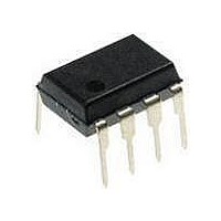
PIC12F1840-I/P Microchip Technology, PIC12F1840-I/P Datasheet - Page 106

PIC12F1840-I/P
Manufacturer Part Number
PIC12F1840-I/P
Description
7 KB Flash, 256 Bytes RAM, 32 MHz Int. Osc, 6 I/0, Enhanced Mid Range Core 8 PDI
Manufacturer
Microchip Technology
Datasheet
1.PIC12F1840-IP.pdf
(382 pages)
Specifications of PIC12F1840-I/P
Processor Series
PIC12F
Core
PIC
Program Memory Type
Flash
Program Memory Size
7 KB
Data Ram Size
256 B
Interface Type
MI2C, SPI, EUSART
Number Of Timers
3
Operating Supply Voltage
1.8 V to 5.5 V
Maximum Operating Temperature
+ 85 C
Mounting Style
Through Hole
Package / Case
PDIP-8
Development Tools By Supplier
MPLAB IDE Software
Minimum Operating Temperature
- 40 C
Lead Free Status / Rohs Status
Lead free / RoHS Compliant
Available stocks
Company
Part Number
Manufacturer
Quantity
Price
Company:
Part Number:
PIC12F1840-I/P
Manufacturer:
MICROCHIP
Quantity:
200
- Current page: 106 of 382
- Download datasheet (4Mb)
PIC12(L)F1840
11.4
When modifying existing data in a program memory
row, and data within that row must be preserved, it must
first be read and saved in a RAM image. Program
memory is modified using the following steps:
1.
2.
3.
4.
5.
6.
7.
8.
TABLE 11-2:
EXAMPLE 11-3:
DS41441B-page 106
* This code block will read 1 word of program memory at the memory address:
*
*
Load the starting address of the row to be mod-
ified.
Read the existing data from the row into a RAM
image.
Modify the RAM image to contain the new data
to be written into program memory.
Load the starting address of the row to be rewrit-
ten.
Erase the program memory row.
Load the write latches with data from the RAM
image.
Initiate a programming operation.
Repeat steps 6 and 7 as many times as required
to reprogram the erased row.
PROG_ADDR_LO (must be 00h-08h) data will be returned in the variables;
PROG_DATA_HI, PROG_DATA_LO
BANKSEL
MOVLW
MOVWF
CLRF
BSF
BCF
BSF
NOP
NOP
BSF
MOVF
MOVWF
MOVF
MOVWF
Modifying Flash Program Memory
8000h-8003h
8007h-8008h
Address
8006h
EEADRL
PROG_ADDR_LO
EEADRL
EEADRH
EECON1,CFGS
INTCON,GIE
EECON1,RD
INTCON,GIE
EEDATL,W
PROG_DATA_LO
EEDATH,W
PROG_DATA_HI
USER ID, DEVICE ID AND CONFIGURATION WORD ACCESS (CFGS = 1)
CONFIGURATION WORD AND DEVICE ID ACCESS
Configuration Words 1 and 2
Device ID/Revision ID
; Select correct Bank
;
; Store LSB of address
; Clear MSB of address
; Select Configuration Space
; Disable interrupts
; Initiate read
; Executed (See
; Ignored (See
; Restore interrupts
; Get LSB of word
; Store in user location
; Get MSB of word
; Store in user location
Function
User IDs
Preliminary
Figure
Figure
11-1)
11.5
Instead of accessing program memory or EEPROM
data memory, the User ID’s, Device ID/Revision ID and
Configuration Words can be accessed when CFGS = 1
in the EECON1 register. This is the region that would
be pointed to by PC<15> = 1, but not all addresses are
accessible. Different access may exist for reads and
writes. Refer to
When read access is initiated on an address outside the
parameters listed in
register pair is cleared.
11-1)
Read Access
User ID, Device ID and
Configuration Word Access
Yes
Yes
Yes
Table
Table
11-2.
2011 Microchip Technology Inc.
11-2, the EEDATH:EEDATL
Write Access
Yes
No
No
Related parts for PIC12F1840-I/P
Image
Part Number
Description
Manufacturer
Datasheet
Request
R

Part Number:
Description:
7 KB Flash, 256 Bytes RAM, 32 MHz Int. Osc, 6 I/0, Enhanced Mid Range Core, Nano
Manufacturer:
Microchip Technology
Datasheet:

Part Number:
Description:
MCU, MPU & DSP Development Tools 8 Bit PIC Develop Microcontroller
Manufacturer:
SchmartBoard
Datasheet:

Part Number:
Description:
7 KB Flash, 256 Bytes RAM, 32 MHz Int. Osc, 6 I/0, Enhanced Mid Range Core 8 DFN
Manufacturer:
Microchip Technology

Part Number:
Description:
7 KB Flash, 256 Bytes RAM, 32 MHz Int. Osc, 6 I/0, Enhanced Mid Range Core 8 SOI
Manufacturer:
Microchip Technology

Part Number:
Description:
7 KB Flash, 256 Bytes RAM, 32 MHz Int. Osc, 6 I/0, Enhanced Mid Range Core, Nano
Manufacturer:
Microchip Technology
Datasheet:

Part Number:
Description:
7 KB Flash, 256 Bytes RAM, 32 MHz Int. Osc, 6 I/0, Enhanced Mid Range Core, Nano
Manufacturer:
Microchip Technology
Datasheet:

Part Number:
Description:
7 KB Flash, 256 Bytes RAM, 32 MHz Int. Osc, 6 I/0, Enhanced Mid Range Core, Nano
Manufacturer:
Microchip Technology
Datasheet:

Part Number:
Description:
7 KB Flash, 256 Bytes RAM, 32 MHz Int. Osc, 6 I/0, Enhanced Mid Range Core, Nano
Manufacturer:
Microchip Technology

Part Number:
Description:
7 KB Flash, 256 Bytes RAM, 32 MHz Int. Osc, 6 I/0, Enhanced Mid Range Core, Nano
Manufacturer:
Microchip Technology

Part Number:
Description:
7 KB Flash, 256 Bytes RAM, 32 MHz Int. Osc, 6 I/0, Enhanced Mid Range Core, Nano
Manufacturer:
Microchip Technology
Datasheet:

Part Number:
Description:
7 KB Flash, 256 Bytes RAM, 32 MHz Int. Osc, 6 I/0, Enhanced Mid Range Core, Nano
Manufacturer:
Microchip Technology
Datasheet:

Part Number:
Description:
Manufacturer:
Microchip Technology Inc.
Datasheet:

Part Number:
Description:
Manufacturer:
Microchip Technology Inc.
Datasheet:


