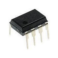
PIC12F1840-I/P Microchip Technology, PIC12F1840-I/P Datasheet - Page 137

PIC12F1840-I/P
Manufacturer Part Number
PIC12F1840-I/P
Description
7 KB Flash, 256 Bytes RAM, 32 MHz Int. Osc, 6 I/0, Enhanced Mid Range Core 8 PDI
Manufacturer
Microchip Technology
Datasheet
1.PIC12F1840-IP.pdf
(382 pages)
Specifications of PIC12F1840-I/P
Processor Series
PIC12F
Core
PIC
Program Memory Type
Flash
Program Memory Size
7 KB
Data Ram Size
256 B
Interface Type
MI2C, SPI, EUSART
Number Of Timers
3
Operating Supply Voltage
1.8 V to 5.5 V
Maximum Operating Temperature
+ 85 C
Mounting Style
Through Hole
Package / Case
PDIP-8
Development Tools By Supplier
MPLAB IDE Software
Minimum Operating Temperature
- 40 C
Lead Free Status / Rohs Status
Lead free / RoHS Compliant
Available stocks
Company
Part Number
Manufacturer
Quantity
Price
Company:
Part Number:
PIC12F1840-I/P
Manufacturer:
MICROCHIP
Quantity:
200
- Current page: 137 of 382
- Download datasheet (4Mb)
16.3
For the ADC to meet its specified accuracy, the charge
holding capacitor (C
charge to the input channel voltage level. The Analog
Input model is shown in
impedance (R
impedance directly affect the time required to charge
the capacitor C
impedance varies over the device voltage (V
to
impedance for analog sources is 10 k. As the
EQUATION 16-1:
2011 Microchip Technology Inc.
The value for T
Solving for T
Assumptions:
Therefore:
Note 1: The reference voltage (V
Figure
V
V
V
Note: Where n = number of bits of the ADC.
2: The charge holding capacitor (C
3: The maximum recommended impedance for analog sources is 10 k. This is required to meet the pin
A/D Acquisition Requirements
AP P LI ED
AP P LI ED
AP P LI ED
16-4.
leakage specification.
T
S
T
A CQ
) and the internal sampling switch (R
C
ACQ
T
:
HOLD
C
C
The
Temperature
can be approximated with the following equations:
=
=
=
=
1
1 e
1 e
=
HOLD
=
=
=
. The sampling switch (R
ACQUISITION TIME EXAMPLE
–
–
–
1.12
4.42µs
–
–
2µs
Amplifier Settling Time
T
2µs
C
10pF 1k
--------------------------
maximum
AMP
) must be allowed to fully
2
–
--------- -
–
-------- -
HOLD
RC
RC
µs
T
Tc
+
n
Figure
+
C
+
1.12µs
+
T
1
1
C
1
=
R
=
T
+
–
IC
C
16-4. The source
=
V
V
+
+
REF
+
+
A PP LIE D
CHOLD
recommended
7k
50°C and external impedance of 10k
Temperature - 25°C
T
R
COFF
) has no effect on the equation, since it cancels itself out.
=
SS
50°C- 25°C
+
+
HOLD
DD
V
10k
R
CHOLD
), refer
S
+
1
) is not discharged after each conversion.
ln(1/511)
Preliminary
SS
SS
–
Hold Capacitor Charging Time
)
)
--------------------------
ln(0.001957)
2
0.05
n
+
0.05µs/°C
1
µs/°C
1
1
source impedance is decreased, the acquisition time
may be decreased. After the analog input channel is
selected (or changed), an A/D acquisition must be
done before the conversion can be started. To calculate
the minimum acquisition time,
used. This equation assumes that 1/2 LSb error is used
(1,024 steps for the ADC). The 1/2 LSb error is the
maximum error allowed for the ADC to meet its
specified resolution.
–
;[1] V
;[2] V
;combining [1] and [2]
CHOLD
CHOLD
5.0V V
PIC12(L)F1840
+
charged to within 1/2 lsb
charge response to V
DD
Temperature Coefficient
Equation 16-1
DS41441B-page 137
APPLIED
may be
Related parts for PIC12F1840-I/P
Image
Part Number
Description
Manufacturer
Datasheet
Request
R

Part Number:
Description:
7 KB Flash, 256 Bytes RAM, 32 MHz Int. Osc, 6 I/0, Enhanced Mid Range Core, Nano
Manufacturer:
Microchip Technology
Datasheet:

Part Number:
Description:
MCU, MPU & DSP Development Tools 8 Bit PIC Develop Microcontroller
Manufacturer:
SchmartBoard
Datasheet:

Part Number:
Description:
7 KB Flash, 256 Bytes RAM, 32 MHz Int. Osc, 6 I/0, Enhanced Mid Range Core 8 DFN
Manufacturer:
Microchip Technology

Part Number:
Description:
7 KB Flash, 256 Bytes RAM, 32 MHz Int. Osc, 6 I/0, Enhanced Mid Range Core 8 SOI
Manufacturer:
Microchip Technology

Part Number:
Description:
7 KB Flash, 256 Bytes RAM, 32 MHz Int. Osc, 6 I/0, Enhanced Mid Range Core, Nano
Manufacturer:
Microchip Technology
Datasheet:

Part Number:
Description:
7 KB Flash, 256 Bytes RAM, 32 MHz Int. Osc, 6 I/0, Enhanced Mid Range Core, Nano
Manufacturer:
Microchip Technology
Datasheet:

Part Number:
Description:
7 KB Flash, 256 Bytes RAM, 32 MHz Int. Osc, 6 I/0, Enhanced Mid Range Core, Nano
Manufacturer:
Microchip Technology
Datasheet:

Part Number:
Description:
7 KB Flash, 256 Bytes RAM, 32 MHz Int. Osc, 6 I/0, Enhanced Mid Range Core, Nano
Manufacturer:
Microchip Technology

Part Number:
Description:
7 KB Flash, 256 Bytes RAM, 32 MHz Int. Osc, 6 I/0, Enhanced Mid Range Core, Nano
Manufacturer:
Microchip Technology

Part Number:
Description:
7 KB Flash, 256 Bytes RAM, 32 MHz Int. Osc, 6 I/0, Enhanced Mid Range Core, Nano
Manufacturer:
Microchip Technology
Datasheet:

Part Number:
Description:
7 KB Flash, 256 Bytes RAM, 32 MHz Int. Osc, 6 I/0, Enhanced Mid Range Core, Nano
Manufacturer:
Microchip Technology
Datasheet:

Part Number:
Description:
Manufacturer:
Microchip Technology Inc.
Datasheet:

Part Number:
Description:
Manufacturer:
Microchip Technology Inc.
Datasheet:


