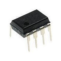
PIC12F1840-I/P Microchip Technology, PIC12F1840-I/P Datasheet - Page 33

PIC12F1840-I/P
Manufacturer Part Number
PIC12F1840-I/P
Description
7 KB Flash, 256 Bytes RAM, 32 MHz Int. Osc, 6 I/0, Enhanced Mid Range Core 8 PDI
Manufacturer
Microchip Technology
Datasheet
1.PIC12F1840-IP.pdf
(382 pages)
Specifications of PIC12F1840-I/P
Processor Series
PIC12F
Core
PIC
Program Memory Type
Flash
Program Memory Size
7 KB
Data Ram Size
256 B
Interface Type
MI2C, SPI, EUSART
Number Of Timers
3
Operating Supply Voltage
1.8 V to 5.5 V
Maximum Operating Temperature
+ 85 C
Mounting Style
Through Hole
Package / Case
PDIP-8
Development Tools By Supplier
MPLAB IDE Software
Minimum Operating Temperature
- 40 C
Lead Free Status / Rohs Status
Lead free / RoHS Compliant
Available stocks
Company
Part Number
Manufacturer
Quantity
Price
Company:
Part Number:
PIC12F1840-I/P
Manufacturer:
MICROCHIP
Quantity:
200
- Current page: 33 of 382
- Download datasheet (4Mb)
TABLE 3-7:
2011 Microchip Technology Inc.
F80h
F81h
F82h
F83h
F84h
F85h
F86h
F87h
F88h
F89h
F8Ah
F8Bh
F8Ch
FE3h
FE4h
FE5h
FE6h
FE7h
FE8h
FE9h
FEAh
FEBh
FECh
FEDh
FEEh
FEFh
Legend:
Note
Address
Bank 31
—
(1)
(1)
(1)
(1)
(1)
(1)
(1)
(1)
(1)
(1)
(1)
(1)
1: These registers can be addressed from any bank.
2: PIC12F1840 only.
INDF0
INDF1
PCL
STATUS
FSR0L
FSR0H
FSR1L
FSR1H
BSR
WREG
PCLATH
INTCON
—
STATUS_
SHAD
WREG_
SHAD
BSR_
SHAD
PCLATH_
SHAD
FSR0L_
SHAD
FSR0H_
SHAD
FSR1L_
SHAD
FSR1H_
SHAD
—
STKPTR
TOSL
TOSH
x = unknown, u = unchanged, q = value depends on condition, - = unimplemented, r = reserved.
Name
Shaded locations are unimplemented, read as ‘0’.
SPECIAL FUNCTION REGISTER SUMMARY (CONTINUED)
Addressing this location uses contents of FSR0H/FSR0L to address data memory
(not a physical register)
Addressing this location uses contents of FSR1H/FSR1L to address data memory
(not a physical register)
Program Counter (PC) Least Significant Byte
Indirect Data Memory Address 0 Low Pointer
Indirect Data Memory Address 0 High Pointer
Indirect Data Memory Address 1 Low Pointer
Indirect Data Memory Address 1 High Pointer
Working Register
Unimplemented
Working Register Shadow
Indirect Data Memory Address 0 Low Pointer Shadow
Indirect Data Memory Address 0 High Pointer Shadow
Indirect Data Memory Address 1 Low Pointer Shadow
Indirect Data Memory Address 1 High Pointer Shadow
Unimplemented
Top-of-Stack Low byte
Bit 7
GIE
—
—
—
—
—
—
—
—
Write Buffer for the upper 7 bits of the Program Counter
Program Counter Latch High Register Shadow
Top-of-Stack High byte
PEIE
Bit 6
—
—
—
—
—
TMR0IE
Bit 5
—
—
—
—
—
Preliminary
Bank Select Register Shadow
Current Stack Pointer
Bit 4
INTE
TO
—
IOCIE
Bit 3
PD
—
BSR<4:0>
Z_SHAD
TMR0IF
Bit 2
Z
PIC12(L)F1840
DC_SHAD
Bit 1
INTF
DC
C_SHAD
IOCIF
Bit 0
C
DS41441B-page 33
xxxx xxxx xxxx xxxx
xxxx xxxx xxxx xxxx
0000 0000 0000 0000
---1 1000 ---q quuu
0000 0000 uuuu uuuu
0000 0000 0000 0000
0000 0000 uuuu uuuu
0000 0000 0000 0000
---0 0000 ---0 0000
0000 0000 uuuu uuuu
-000 0000 -000 0000
0000 000x 0000 000u
---- -xxx ---- -uuu
0000 0000 uuuu uuuu
---x xxxx ---u uuuu
-xxx xxxx uuuu uuuu
xxxx xxxx uuuu uuuu
xxxx xxxx uuuu uuuu
xxxx xxxx uuuu uuuu
xxxx xxxx uuuu uuuu
---1 1111 ---1 1111
xxxx xxxx uuuu uuuu
-xxx xxxx -uuu uuuu
POR, BOR
Value on
—
—
Value on all
Resets
other
—
—
Related parts for PIC12F1840-I/P
Image
Part Number
Description
Manufacturer
Datasheet
Request
R

Part Number:
Description:
7 KB Flash, 256 Bytes RAM, 32 MHz Int. Osc, 6 I/0, Enhanced Mid Range Core, Nano
Manufacturer:
Microchip Technology
Datasheet:

Part Number:
Description:
MCU, MPU & DSP Development Tools 8 Bit PIC Develop Microcontroller
Manufacturer:
SchmartBoard
Datasheet:

Part Number:
Description:
7 KB Flash, 256 Bytes RAM, 32 MHz Int. Osc, 6 I/0, Enhanced Mid Range Core 8 DFN
Manufacturer:
Microchip Technology

Part Number:
Description:
7 KB Flash, 256 Bytes RAM, 32 MHz Int. Osc, 6 I/0, Enhanced Mid Range Core 8 SOI
Manufacturer:
Microchip Technology

Part Number:
Description:
7 KB Flash, 256 Bytes RAM, 32 MHz Int. Osc, 6 I/0, Enhanced Mid Range Core, Nano
Manufacturer:
Microchip Technology
Datasheet:

Part Number:
Description:
7 KB Flash, 256 Bytes RAM, 32 MHz Int. Osc, 6 I/0, Enhanced Mid Range Core, Nano
Manufacturer:
Microchip Technology
Datasheet:

Part Number:
Description:
7 KB Flash, 256 Bytes RAM, 32 MHz Int. Osc, 6 I/0, Enhanced Mid Range Core, Nano
Manufacturer:
Microchip Technology
Datasheet:

Part Number:
Description:
7 KB Flash, 256 Bytes RAM, 32 MHz Int. Osc, 6 I/0, Enhanced Mid Range Core, Nano
Manufacturer:
Microchip Technology

Part Number:
Description:
7 KB Flash, 256 Bytes RAM, 32 MHz Int. Osc, 6 I/0, Enhanced Mid Range Core, Nano
Manufacturer:
Microchip Technology

Part Number:
Description:
7 KB Flash, 256 Bytes RAM, 32 MHz Int. Osc, 6 I/0, Enhanced Mid Range Core, Nano
Manufacturer:
Microchip Technology
Datasheet:

Part Number:
Description:
7 KB Flash, 256 Bytes RAM, 32 MHz Int. Osc, 6 I/0, Enhanced Mid Range Core, Nano
Manufacturer:
Microchip Technology
Datasheet:

Part Number:
Description:
Manufacturer:
Microchip Technology Inc.
Datasheet:

Part Number:
Description:
Manufacturer:
Microchip Technology Inc.
Datasheet:


