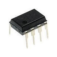
PIC12F1840-I/P Microchip Technology, PIC12F1840-I/P Datasheet - Page 163

PIC12F1840-I/P
Manufacturer Part Number
PIC12F1840-I/P
Description
7 KB Flash, 256 Bytes RAM, 32 MHz Int. Osc, 6 I/0, Enhanced Mid Range Core 8 PDI
Manufacturer
Microchip Technology
Datasheet
1.PIC12F1840-IP.pdf
(382 pages)
Specifications of PIC12F1840-I/P
Processor Series
PIC12F
Core
PIC
Program Memory Type
Flash
Program Memory Size
7 KB
Data Ram Size
256 B
Interface Type
MI2C, SPI, EUSART
Number Of Timers
3
Operating Supply Voltage
1.8 V to 5.5 V
Maximum Operating Temperature
+ 85 C
Mounting Style
Through Hole
Package / Case
PDIP-8
Development Tools By Supplier
MPLAB IDE Software
Minimum Operating Temperature
- 40 C
Lead Free Status / Rohs Status
Lead free / RoHS Compliant
Available stocks
Company
Part Number
Manufacturer
Quantity
Price
Company:
Part Number:
PIC12F1840-I/P
Manufacturer:
MICROCHIP
Quantity:
200
- Current page: 163 of 382
- Download datasheet (4Mb)
21.0
The Timer1 module is a 16-bit timer/counter with the
following features:
• 16-bit timer/counter register pair (TMR1H:TMR1L)
• Programmable internal or external clock source
• 2-bit prescaler
• Dedicated 32 kHz oscillator circuit
• Optionally synchronized comparator out
• Multiple Timer1 gate (count enable) sources
• Interrupt on overflow
• Wake-up on overflow (external clock,
• Time base for the Capture/Compare function
• Special Event Trigger (with ECCP)
• Selectable Gate Source Polarity
FIGURE 21-1:
2011 Microchip Technology Inc.
Asynchronous mode only)
From Timer0
T1G
Overflow
Reserved
T1GSS<1:0>
Note 1: ST Buffer is high speed type when using T1CKI.
TIMER1 MODULE WITH GATE
CONTROL
2: Timer1 register increments on rising edge.
3: Synchronize does not operate while in Sleep.
T1OSCEN
T1OSO
T1GPOL
T1CKI
T1OSI
Set flag bit
TMR1IF on
Overflow
00
10
TIMER1 BLOCK DIAGRAM
01
TMR1ON
T1GTM
T1OSC
TMR1H
EN
OUT
TMR1
(1)
T1G_IN
(2)
D
R
CK
TMR1L
Q
Q
1
0
Preliminary
TMR1CS<1:0>
Cap. Sensing
0
1
Oscillator
T1GGO/DONE
Q
Internal
Internal
F
OSC
Clock
Clock
F
OSC
EN
/4
D
• Gate Toggle Mode
• Gate Single-pulse Mode
• Gate Value Status
• Gate Event Interrupt
Figure 21-1
Single Pulse
Acq. Control
T1CLK
11
10
01
00
T1GSPM
T1CKPS<1:0>
T1SYNC
Prescaler
1, 2, 4, 8
TMR1ON
is a block diagram of the Timer1 module.
0
1
To Clock Switching Modules
2
0
1
PIC12(L)F1840
Internal
F
Clock
T1GVAL
OSC
TMR1GE
/2
Q1
Synchronized
Synchronize
Interrupt
clock input
D
EN
det
det
Sleep input
Q
(3)
To Comparator Module
DS41441B-page 163
Set
TMR1GIF
T1GCON
Data Bus
RD
Related parts for PIC12F1840-I/P
Image
Part Number
Description
Manufacturer
Datasheet
Request
R

Part Number:
Description:
7 KB Flash, 256 Bytes RAM, 32 MHz Int. Osc, 6 I/0, Enhanced Mid Range Core, Nano
Manufacturer:
Microchip Technology
Datasheet:

Part Number:
Description:
MCU, MPU & DSP Development Tools 8 Bit PIC Develop Microcontroller
Manufacturer:
SchmartBoard
Datasheet:

Part Number:
Description:
7 KB Flash, 256 Bytes RAM, 32 MHz Int. Osc, 6 I/0, Enhanced Mid Range Core 8 DFN
Manufacturer:
Microchip Technology

Part Number:
Description:
7 KB Flash, 256 Bytes RAM, 32 MHz Int. Osc, 6 I/0, Enhanced Mid Range Core 8 SOI
Manufacturer:
Microchip Technology

Part Number:
Description:
7 KB Flash, 256 Bytes RAM, 32 MHz Int. Osc, 6 I/0, Enhanced Mid Range Core, Nano
Manufacturer:
Microchip Technology
Datasheet:

Part Number:
Description:
7 KB Flash, 256 Bytes RAM, 32 MHz Int. Osc, 6 I/0, Enhanced Mid Range Core, Nano
Manufacturer:
Microchip Technology
Datasheet:

Part Number:
Description:
7 KB Flash, 256 Bytes RAM, 32 MHz Int. Osc, 6 I/0, Enhanced Mid Range Core, Nano
Manufacturer:
Microchip Technology
Datasheet:

Part Number:
Description:
7 KB Flash, 256 Bytes RAM, 32 MHz Int. Osc, 6 I/0, Enhanced Mid Range Core, Nano
Manufacturer:
Microchip Technology

Part Number:
Description:
7 KB Flash, 256 Bytes RAM, 32 MHz Int. Osc, 6 I/0, Enhanced Mid Range Core, Nano
Manufacturer:
Microchip Technology

Part Number:
Description:
7 KB Flash, 256 Bytes RAM, 32 MHz Int. Osc, 6 I/0, Enhanced Mid Range Core, Nano
Manufacturer:
Microchip Technology
Datasheet:

Part Number:
Description:
7 KB Flash, 256 Bytes RAM, 32 MHz Int. Osc, 6 I/0, Enhanced Mid Range Core, Nano
Manufacturer:
Microchip Technology
Datasheet:

Part Number:
Description:
Manufacturer:
Microchip Technology Inc.
Datasheet:

Part Number:
Description:
Manufacturer:
Microchip Technology Inc.
Datasheet:


