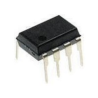
PIC12F1840-I/P Microchip Technology, PIC12F1840-I/P Datasheet - Page 337

PIC12F1840-I/P
Manufacturer Part Number
PIC12F1840-I/P
Description
7 KB Flash, 256 Bytes RAM, 32 MHz Int. Osc, 6 I/0, Enhanced Mid Range Core 8 PDI
Manufacturer
Microchip Technology
Datasheet
1.PIC12F1840-IP.pdf
(382 pages)
Specifications of PIC12F1840-I/P
Processor Series
PIC12F
Core
PIC
Program Memory Type
Flash
Program Memory Size
7 KB
Data Ram Size
256 B
Interface Type
MI2C, SPI, EUSART
Number Of Timers
3
Operating Supply Voltage
1.8 V to 5.5 V
Maximum Operating Temperature
+ 85 C
Mounting Style
Through Hole
Package / Case
PDIP-8
Development Tools By Supplier
MPLAB IDE Software
Minimum Operating Temperature
- 40 C
Lead Free Status / Rohs Status
Lead free / RoHS Compliant
Available stocks
Company
Part Number
Manufacturer
Quantity
Price
Company:
Part Number:
PIC12F1840-I/P
Manufacturer:
MICROCHIP
Quantity:
200
- Current page: 337 of 382
- Download datasheet (4Mb)
TABLE 30-2:
TABLE 30-3:
2011 Microchip Technology Inc.
Standard Operating Conditions (unless otherwise stated)
Operating Temperature
OS08
OS08A MF
OS09
OS10*
Note 1: Instruction cycle period (T
F10
F11
F12
F13*
Param
Param
No.
No.
*
†
2: To ensure these oscillator frequency tolerances, V
3: By design.
*
† Data in “Typ” column is at 3V, 25C unless otherwise stated. These parameters are for design guidance
HF
LF
T
These parameters are characterized but not tested.
Data in “Typ” column is at 3.0V, 25°C unless otherwise stated. These parameters are for design guidance only and are not
tested.
characterization data for that particular oscillator type under standard operating conditions with the device executing code.
Exceeding these specified limits may result in an unstable oscillator operation and/or higher than expected current con-
sumption. All devices are tested to operate at “min” values with an external clock applied to the OSC1 pin. When an exter-
nal clock input is used, the “max” cycle time limit is “DC” (no clock) for all devices.
possible. 0.1 F and 0.01 F values in parallel are recommended.
IOSC ST
F
F
T
Sym.
Sym.
OSC
OSC
OSC
SYS
RC
CLK
These parameters are characterized but not tested.
only and are not tested.
OSC
Oscillator Frequency Range
On-Chip VCO System Frequency
PLL Start-up Time (Lock Time)
CLKOUT Stability (Jitter)
OSCILLATOR PARAMETERS
PLL CLOCK TIMING SPECIFICATIONS (V
Internal Calibrated HFINTOSC
Frequency
Internal Calibrated MFINTOSC
Frequency
Internal LFINTOSC Frequency
HFINTOSC
Wake-up from Sleep Start-up Time
MFINTOSC
Wake-up from Sleep Start-up Time
-40°C T
Characteristic
(2)
(2)
Characteristic
CY
A
+125°C
) equals four times the input oscillator time base period. All specified values are based on
Preliminary
Tolerance
Freq.
2%
3%
5%
2%
3%
5%
DD
—
—
—
and V
SS
Min.
21.5
—
—
—
—
—
—
—
—
-0.25%
must be capacitively decoupled as close to the device as
Min.
16
—
DD
4
Typ†
16.0
16.0
16.0
= 2.7V TO 5.5V)
500
500
500
31
20
5
Typ†
Max.
—
—
—
—
40.5
30
—
—
—
—
—
—
8
PIC12(L)F1840
Units
MHz
MHz
MHz
kHz
kHz
kHz
kHz
s
s
+0.25%
Max.
32
8
2
0°C T
60°C T
-40°C T
0°C T
60°C T
-40°C T
-40°C T
Units
MHz
MHz
ms
A
A
%
A
A
DS41441B-page 337
Conditions
+60°C, V
+60°C, V
A
A
A
+85°C, V
+85°C, V
+125°C
+125°C
+125°C
Conditions
DD
DD
DD
DD
2.5V
2.5V
2.5V
2.5V
Related parts for PIC12F1840-I/P
Image
Part Number
Description
Manufacturer
Datasheet
Request
R

Part Number:
Description:
7 KB Flash, 256 Bytes RAM, 32 MHz Int. Osc, 6 I/0, Enhanced Mid Range Core, Nano
Manufacturer:
Microchip Technology
Datasheet:

Part Number:
Description:
MCU, MPU & DSP Development Tools 8 Bit PIC Develop Microcontroller
Manufacturer:
SchmartBoard
Datasheet:

Part Number:
Description:
7 KB Flash, 256 Bytes RAM, 32 MHz Int. Osc, 6 I/0, Enhanced Mid Range Core 8 DFN
Manufacturer:
Microchip Technology

Part Number:
Description:
7 KB Flash, 256 Bytes RAM, 32 MHz Int. Osc, 6 I/0, Enhanced Mid Range Core 8 SOI
Manufacturer:
Microchip Technology

Part Number:
Description:
7 KB Flash, 256 Bytes RAM, 32 MHz Int. Osc, 6 I/0, Enhanced Mid Range Core, Nano
Manufacturer:
Microchip Technology
Datasheet:

Part Number:
Description:
7 KB Flash, 256 Bytes RAM, 32 MHz Int. Osc, 6 I/0, Enhanced Mid Range Core, Nano
Manufacturer:
Microchip Technology
Datasheet:

Part Number:
Description:
7 KB Flash, 256 Bytes RAM, 32 MHz Int. Osc, 6 I/0, Enhanced Mid Range Core, Nano
Manufacturer:
Microchip Technology
Datasheet:

Part Number:
Description:
7 KB Flash, 256 Bytes RAM, 32 MHz Int. Osc, 6 I/0, Enhanced Mid Range Core, Nano
Manufacturer:
Microchip Technology

Part Number:
Description:
7 KB Flash, 256 Bytes RAM, 32 MHz Int. Osc, 6 I/0, Enhanced Mid Range Core, Nano
Manufacturer:
Microchip Technology

Part Number:
Description:
7 KB Flash, 256 Bytes RAM, 32 MHz Int. Osc, 6 I/0, Enhanced Mid Range Core, Nano
Manufacturer:
Microchip Technology
Datasheet:

Part Number:
Description:
7 KB Flash, 256 Bytes RAM, 32 MHz Int. Osc, 6 I/0, Enhanced Mid Range Core, Nano
Manufacturer:
Microchip Technology
Datasheet:

Part Number:
Description:
Manufacturer:
Microchip Technology Inc.
Datasheet:

Part Number:
Description:
Manufacturer:
Microchip Technology Inc.
Datasheet:


