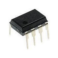
PIC12F1840-I/P Microchip Technology, PIC12F1840-I/P Datasheet - Page 195

PIC12F1840-I/P
Manufacturer Part Number
PIC12F1840-I/P
Description
7 KB Flash, 256 Bytes RAM, 32 MHz Int. Osc, 6 I/0, Enhanced Mid Range Core 8 PDI
Manufacturer
Microchip Technology
Datasheet
1.PIC12F1840-IP.pdf
(382 pages)
Specifications of PIC12F1840-I/P
Processor Series
PIC12F
Core
PIC
Program Memory Type
Flash
Program Memory Size
7 KB
Data Ram Size
256 B
Interface Type
MI2C, SPI, EUSART
Number Of Timers
3
Operating Supply Voltage
1.8 V to 5.5 V
Maximum Operating Temperature
+ 85 C
Mounting Style
Through Hole
Package / Case
PDIP-8
Development Tools By Supplier
MPLAB IDE Software
Minimum Operating Temperature
- 40 C
Lead Free Status / Rohs Status
Lead free / RoHS Compliant
Available stocks
Company
Part Number
Manufacturer
Quantity
Price
Company:
Part Number:
PIC12F1840-I/P
Manufacturer:
MICROCHIP
Quantity:
200
- Current page: 195 of 382
- Download datasheet (4Mb)
24.3.2
The following steps should be taken when configuring
the CCP1 module for standard PWM operation:
1.
2.
3.
4.
5.
6.
24.3.3
The PWM period is specified by the PR2 register of
Timer2. The PWM period can be calculated using the
formula of
EQUATION 24-1:
2011 Microchip Technology Inc.
Note:
Disable the CCP1 pin output driver by setting
the associated TRIS bit.
Load the PR2 register with the PWM period
value.
Configure the CCP1 module for the PWM mode
by loading the CCP1CON register with the
appropriate values.
Load the CCPR1L register and the DC1B1 bits
of the CCP1CON register, with the PWM duty
cycle value.
Configure and start Timer2:
• Clear the TMR2IF interrupt flag bit of the
• Configure the T2CKPS bits of the T2CON
• Enable the Timer by setting the TMR2ON
Enable PWM output pin:
• Wait until the Timer overflows and the
• Enable the CCP1 pin output driver by clear-
Note 1:
PWM Period
PIR1 register. See Note below.
register with the Timer prescale value.
bit of the T2CON register.
TMR2IF bit of the PIR1 register is set. See
Note below.
ing the associated TRIS bit.
Equation
SETUP FOR PWM OPERATION
In order to send a complete duty cycle and
period on the first PWM output, the above
steps must be included in the setup
sequence. If it is not critical to start with a
complete PWM signal on the first output,
then step 6 may be ignored.
PWM PERIOD
T
OSC
=
24-1.
(TMR2 Prescale Value)
PWM PERIOD
= 1/F
PR2
OSC
+
1
4 T
OSC
Preliminary
When TMR2 is equal to PR2, the following three events
occur on the next increment cycle:
• TMR2 is cleared
• The CCP1 pin is set. (Exception: If the PWM duty
• The PWM duty cycle is latched from CCPR1L into
24.3.4
The PWM duty cycle is specified by writing a 10-bit
value to multiple registers: CCPR1L register and
DC1B<1:0> bits of the CCP1CON register. The
CCPR1L contains the eight MSbs and the DC1B<1:0>
bits of the CCP1CON register contain the two LSbs.
CCPR1L and DC1B<1:0> bits of the CCP1CON
register can be written to at any time. The duty cycle
value is not latched into CCPR1H until after the period
completes (i.e., a match between PR2 and TMR2
registers occurs). While using the PWM, the CCPR1H
register is read-only.
Equation 24-2
width.
Equation 24-3
ratio.
EQUATION 24-2:
EQUATION 24-3:
The CCPR1H register and a 2-bit internal latch are
used to double buffer the PWM duty cycle. This double
buffering is essential for glitchless PWM operation.
The 8-bit timer TMR2 register is concatenated with
either the 2-bit internal system clock (F
the prescaler, to create the 10-bit time base. The system
clock is used if the Timer2 prescaler is set to 1:1.
When the 10-bit time base matches the CCPR1H and
2-bit latch, then the CCP1 pin is cleared (see
Figure
cycle = 0%, the pin will not be set.)
CCPR1H.
Note:
Duty Cycle Ratio
Pulse Width
24-4).
The Timer postscaler (see
“Timer2
determination of the PWM frequency.
PWM DUTY CYCLE
is used to calculate the PWM duty cycle
is used to calculate the PWM pulse
PIC12(L)F1840
=
T
=
CCPR1L:CCP1CON<5:4>
OSC
Operation”) is not used in the
PULSE WIDTH
DUTY CYCLE RATIO
---------------------------------------------------------------------- -
CCPR1L:CCP1CON<5:4>
(TMR2 Prescale Value)
4 PR2
DS41441B-page 195
+
OSC
1
Section 22.1
), or 2 bits of
Related parts for PIC12F1840-I/P
Image
Part Number
Description
Manufacturer
Datasheet
Request
R

Part Number:
Description:
7 KB Flash, 256 Bytes RAM, 32 MHz Int. Osc, 6 I/0, Enhanced Mid Range Core, Nano
Manufacturer:
Microchip Technology
Datasheet:

Part Number:
Description:
MCU, MPU & DSP Development Tools 8 Bit PIC Develop Microcontroller
Manufacturer:
SchmartBoard
Datasheet:

Part Number:
Description:
7 KB Flash, 256 Bytes RAM, 32 MHz Int. Osc, 6 I/0, Enhanced Mid Range Core 8 DFN
Manufacturer:
Microchip Technology

Part Number:
Description:
7 KB Flash, 256 Bytes RAM, 32 MHz Int. Osc, 6 I/0, Enhanced Mid Range Core 8 SOI
Manufacturer:
Microchip Technology

Part Number:
Description:
7 KB Flash, 256 Bytes RAM, 32 MHz Int. Osc, 6 I/0, Enhanced Mid Range Core, Nano
Manufacturer:
Microchip Technology
Datasheet:

Part Number:
Description:
7 KB Flash, 256 Bytes RAM, 32 MHz Int. Osc, 6 I/0, Enhanced Mid Range Core, Nano
Manufacturer:
Microchip Technology
Datasheet:

Part Number:
Description:
7 KB Flash, 256 Bytes RAM, 32 MHz Int. Osc, 6 I/0, Enhanced Mid Range Core, Nano
Manufacturer:
Microchip Technology
Datasheet:

Part Number:
Description:
7 KB Flash, 256 Bytes RAM, 32 MHz Int. Osc, 6 I/0, Enhanced Mid Range Core, Nano
Manufacturer:
Microchip Technology

Part Number:
Description:
7 KB Flash, 256 Bytes RAM, 32 MHz Int. Osc, 6 I/0, Enhanced Mid Range Core, Nano
Manufacturer:
Microchip Technology

Part Number:
Description:
7 KB Flash, 256 Bytes RAM, 32 MHz Int. Osc, 6 I/0, Enhanced Mid Range Core, Nano
Manufacturer:
Microchip Technology
Datasheet:

Part Number:
Description:
7 KB Flash, 256 Bytes RAM, 32 MHz Int. Osc, 6 I/0, Enhanced Mid Range Core, Nano
Manufacturer:
Microchip Technology
Datasheet:

Part Number:
Description:
Manufacturer:
Microchip Technology Inc.
Datasheet:

Part Number:
Description:
Manufacturer:
Microchip Technology Inc.
Datasheet:


