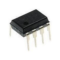
PIC12F1840-I/P Microchip Technology, PIC12F1840-I/P Datasheet - Page 143

PIC12F1840-I/P
Manufacturer Part Number
PIC12F1840-I/P
Description
7 KB Flash, 256 Bytes RAM, 32 MHz Int. Osc, 6 I/0, Enhanced Mid Range Core 8 PDI
Manufacturer
Microchip Technology
Datasheet
1.PIC12F1840-IP.pdf
(382 pages)
Specifications of PIC12F1840-I/P
Processor Series
PIC12F
Core
PIC
Program Memory Type
Flash
Program Memory Size
7 KB
Data Ram Size
256 B
Interface Type
MI2C, SPI, EUSART
Number Of Timers
3
Operating Supply Voltage
1.8 V to 5.5 V
Maximum Operating Temperature
+ 85 C
Mounting Style
Through Hole
Package / Case
PDIP-8
Development Tools By Supplier
MPLAB IDE Software
Minimum Operating Temperature
- 40 C
Lead Free Status / Rohs Status
Lead free / RoHS Compliant
Available stocks
Company
Part Number
Manufacturer
Quantity
Price
Company:
Part Number:
PIC12F1840-I/P
Manufacturer:
MICROCHIP
Quantity:
200
- Current page: 143 of 382
- Download datasheet (4Mb)
17.4
In order for the DAC module to consume the least
amount of power, one of the two voltage reference input
sources to the resistor ladder must be disconnected.
Either the positive voltage source, (V
negative voltage source, (V
The negative voltage source is disabled by setting the
DACLPS bit in the DACCON0 register. Clearing the
DACLPS bit in the DACCON0 register disables the
positive voltage source.
17.4.1
The DAC output voltage can be set to V
the least amount of power consumption by performing
the following:
• Clearing the DACEN bit in the DACCON0 register.
• Setting the DACLPS bit in the DACCON0 register.
• Configuring the DACPSS bits to the proper
• Configuring the DACR<4:0> bits to ‘11111’ in the
FIGURE 17-3:
17.5
When the device wakes up from Sleep through an
interrupt or a Watchdog Timer time-out, the contents of
the DACCON0 register are not affected. To minimize
current consumption in Sleep mode, the voltage
reference should be disabled.
17.6
A device Reset affects the following:
• DAC is disabled.
• DAC output voltage is removed from the
• The DACR<4:0> range select bits are cleared.
2011 Microchip Technology Inc.
positive source.
DACCON1 register.
DACOUT pin.
V
V
SOURCE
Output Clamped to Positive Voltage Source
SOURCE
DACEN = 0
DACLPS = 1
Low-Power Voltage State
Operation During Sleep
Effects of a Reset
OUTPUT CLAMPED TO POSITIVE
VOLTAGE SOURCE
+
-
OUTPUT VOLTAGE CLAMPING EXAMPLES
SOURCE
R
R
R
DACR<4:0> = 11111
DAC Voltage Ladder
(see
-) can be disabled.
SOURCE
Figure
SOURCE
+), or the
17-1)
+ with
Preliminary
This is also the method used to output the voltage level
from the FVR to an output pin. See
“Operation During Sleep”
Reference
17.4.2
The DAC output voltage can be set to V
the least amount of power consumption by performing
the following:
• Clearing the DACEN bit in the DACCON0 register.
• Clearing the DACLPS bit in the DACCON0 register.
• Configuring the DACR<4:0> bits to ‘00000’ in the
This allows the comparator to detect a zero-crossing
while not consuming additional current through the DAC
module.
Reference
V
V
Output Clamped to Negative Voltage Source
SOURCE
SOURCE
DACCON1 register.
DACEN = 0
DACLPS = 0
+
-
Figure 17-3
Figure 17-3
OUTPUT CLAMPED TO NEGATIVE
VOLTAGE SOURCE
PIC12(L)F1840
for output clamping examples.
for output clamping examples.
R
R
R
for more information.
DACR<4:0> = 00000
DAC Voltage Ladder
(see
Figure
DS41441B-page 143
SOURCE
Section 17.5
17-1)
- with
Related parts for PIC12F1840-I/P
Image
Part Number
Description
Manufacturer
Datasheet
Request
R

Part Number:
Description:
7 KB Flash, 256 Bytes RAM, 32 MHz Int. Osc, 6 I/0, Enhanced Mid Range Core, Nano
Manufacturer:
Microchip Technology
Datasheet:

Part Number:
Description:
MCU, MPU & DSP Development Tools 8 Bit PIC Develop Microcontroller
Manufacturer:
SchmartBoard
Datasheet:

Part Number:
Description:
7 KB Flash, 256 Bytes RAM, 32 MHz Int. Osc, 6 I/0, Enhanced Mid Range Core 8 DFN
Manufacturer:
Microchip Technology

Part Number:
Description:
7 KB Flash, 256 Bytes RAM, 32 MHz Int. Osc, 6 I/0, Enhanced Mid Range Core 8 SOI
Manufacturer:
Microchip Technology

Part Number:
Description:
7 KB Flash, 256 Bytes RAM, 32 MHz Int. Osc, 6 I/0, Enhanced Mid Range Core, Nano
Manufacturer:
Microchip Technology
Datasheet:

Part Number:
Description:
7 KB Flash, 256 Bytes RAM, 32 MHz Int. Osc, 6 I/0, Enhanced Mid Range Core, Nano
Manufacturer:
Microchip Technology
Datasheet:

Part Number:
Description:
7 KB Flash, 256 Bytes RAM, 32 MHz Int. Osc, 6 I/0, Enhanced Mid Range Core, Nano
Manufacturer:
Microchip Technology
Datasheet:

Part Number:
Description:
7 KB Flash, 256 Bytes RAM, 32 MHz Int. Osc, 6 I/0, Enhanced Mid Range Core, Nano
Manufacturer:
Microchip Technology

Part Number:
Description:
7 KB Flash, 256 Bytes RAM, 32 MHz Int. Osc, 6 I/0, Enhanced Mid Range Core, Nano
Manufacturer:
Microchip Technology

Part Number:
Description:
7 KB Flash, 256 Bytes RAM, 32 MHz Int. Osc, 6 I/0, Enhanced Mid Range Core, Nano
Manufacturer:
Microchip Technology
Datasheet:

Part Number:
Description:
7 KB Flash, 256 Bytes RAM, 32 MHz Int. Osc, 6 I/0, Enhanced Mid Range Core, Nano
Manufacturer:
Microchip Technology
Datasheet:

Part Number:
Description:
Manufacturer:
Microchip Technology Inc.
Datasheet:

Part Number:
Description:
Manufacturer:
Microchip Technology Inc.
Datasheet:


