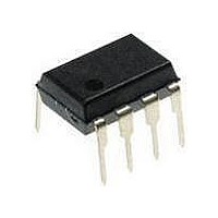
PIC12F1840-I/P Microchip Technology, PIC12F1840-I/P Datasheet - Page 332

PIC12F1840-I/P
Manufacturer Part Number
PIC12F1840-I/P
Description
7 KB Flash, 256 Bytes RAM, 32 MHz Int. Osc, 6 I/0, Enhanced Mid Range Core 8 PDI
Manufacturer
Microchip Technology
Datasheet
1.PIC12F1840-IP.pdf
(382 pages)
Specifications of PIC12F1840-I/P
Processor Series
PIC12F
Core
PIC
Program Memory Type
Flash
Program Memory Size
7 KB
Data Ram Size
256 B
Interface Type
MI2C, SPI, EUSART
Number Of Timers
3
Operating Supply Voltage
1.8 V to 5.5 V
Maximum Operating Temperature
+ 85 C
Mounting Style
Through Hole
Package / Case
PDIP-8
Development Tools By Supplier
MPLAB IDE Software
Minimum Operating Temperature
- 40 C
Lead Free Status / Rohs Status
Lead free / RoHS Compliant
Available stocks
Company
Part Number
Manufacturer
Quantity
Price
Company:
Part Number:
PIC12F1840-I/P
Manufacturer:
MICROCHIP
Quantity:
200
- Current page: 332 of 382
- Download datasheet (4Mb)
PIC12(L)F1840
30.4
DS41441B-page 332
D030
D030A
D031
D032
D033
D040
D040A
D041
D042
D043A
D043B
D060
D061
D070*
D080
D090
D101*
D101A* C
Note 1: In RC oscillator configuration, the OSC1/CLKIN pin is a Schmitt Trigger input. It is not recommended to use an external
Param
No.
*
†
2: Negative current is defined as current sourced by the pin.
3: The leakage current on the MCLR pin is strongly dependent on the applied voltage level. The specified levels represent
4: Including OSC2 in CLKOUT mode.
DC Characteristics: PIC12(L)F1840-I/E
V
V
I
I
V
V
COSC2 OSC2 pin
These parameters are characterized but not tested.
Data in “Typ” column is at 3.0V, 25°C unless otherwise stated. These parameters are for design guidance only and are
not tested.
clock in RC mode.
normal operating conditions. Higher leakage current may be measured at different input voltages.
IL
PUR
Sym.
OL
OH
IL
IH
IO
DC CHARACTERISTICS
Input Low Voltage
I/O PORT:
MCLR, OSC1 (RC mode)
OSC1 (HS mode)
Input High Voltage
I/O ports:
MCLR
OSC1 (HS mode)
OSC1 (RC mode)
Input Leakage Current
I/O ports
MCLR
Weak Pull-up Current
Output Low Voltage
I/O ports
Output High Voltage
I/O ports
Capacitive Loading Specs on Output Pins
All I/O pins
with TTL buffer
with TTL buffer
with I
with SMBus levels
with Schmitt Trigger buffer
with I
with SMBus levels
with Schmitt Trigger buffer
(3)
Characteristic
2
2
C™ levels
C™ levels
(4)
(4)
(2)
(1)
Standard Operating Conditions (unless otherwise stated)
Operating temperature -40°C T
0.25 V
V
0.8 V
0.7 V
0.8 V
0.7 V
0.9 V
DD
Min.
2.0
0.8
2.1
Preliminary
—
—
—
—
—
—
—
—
—
25
25
—
—
—
- 0.7
DD
DD
DD
DD
DD
DD
+
Typ†
± 50
100
140
± 5
± 5
—
—
—
—
—
—
—
—
—
—
—
—
—
—
—
—
—
—
—
—
-40°C T
0.15 V
0.2 V
0.3 V
0.2 V
0.3 V
± 1000
± 125
± 200
Max.
200
300
0.8
0.8
0.6
15
50
—
—
—
—
—
—
—
—
—
—
DD
DD
DD
DD
DD
A
A
+85°C for industrial
+125°C for extended
Units
A
nA
nA
nA
pF
pF
V
V
V
V
V
V
V
V
V
V
V
V
V
V
V
V
V
4.5V V
1.8V V
2.0V V
2.7V V
4.5V V
1.8V V
2.0V V
2.7V V
(Note 1)
V
impedance at 85°C
125°C
V
V
V
I
I
I
I
I
I
In XT, HS and LP modes when
external clock is used to drive
OSC1
OL
OL
OL
OH
OH
OH
SS
SS
DD
DD
2011 Microchip Technology Inc.
= 8mA, V
= 6mA, V
= 1.8mA, V
= 3.5mA, V
= 3mA, V
= 1mA, V
V
V
= 3.3V, V
= 5.0V, V
PIN
PIN
DD
DD
DD
DD
DD
DD
DD
DD
5.5V
V
V
Conditions
5.5V
4.5V
5.5V
5.5V
4.5V
5.5V
5.5V
DD
DD
DD
DD
PIN
PIN
DD
DD
DD
DD
= 5V
= 3.3V
= 3.3V
= 1.8V
, Pin at high-
= V
= V
= 1.8V
at 85°C
= 5V
SS
SS
Related parts for PIC12F1840-I/P
Image
Part Number
Description
Manufacturer
Datasheet
Request
R

Part Number:
Description:
7 KB Flash, 256 Bytes RAM, 32 MHz Int. Osc, 6 I/0, Enhanced Mid Range Core, Nano
Manufacturer:
Microchip Technology
Datasheet:

Part Number:
Description:
MCU, MPU & DSP Development Tools 8 Bit PIC Develop Microcontroller
Manufacturer:
SchmartBoard
Datasheet:

Part Number:
Description:
7 KB Flash, 256 Bytes RAM, 32 MHz Int. Osc, 6 I/0, Enhanced Mid Range Core 8 DFN
Manufacturer:
Microchip Technology

Part Number:
Description:
7 KB Flash, 256 Bytes RAM, 32 MHz Int. Osc, 6 I/0, Enhanced Mid Range Core 8 SOI
Manufacturer:
Microchip Technology

Part Number:
Description:
7 KB Flash, 256 Bytes RAM, 32 MHz Int. Osc, 6 I/0, Enhanced Mid Range Core, Nano
Manufacturer:
Microchip Technology
Datasheet:

Part Number:
Description:
7 KB Flash, 256 Bytes RAM, 32 MHz Int. Osc, 6 I/0, Enhanced Mid Range Core, Nano
Manufacturer:
Microchip Technology
Datasheet:

Part Number:
Description:
7 KB Flash, 256 Bytes RAM, 32 MHz Int. Osc, 6 I/0, Enhanced Mid Range Core, Nano
Manufacturer:
Microchip Technology
Datasheet:

Part Number:
Description:
7 KB Flash, 256 Bytes RAM, 32 MHz Int. Osc, 6 I/0, Enhanced Mid Range Core, Nano
Manufacturer:
Microchip Technology

Part Number:
Description:
7 KB Flash, 256 Bytes RAM, 32 MHz Int. Osc, 6 I/0, Enhanced Mid Range Core, Nano
Manufacturer:
Microchip Technology

Part Number:
Description:
7 KB Flash, 256 Bytes RAM, 32 MHz Int. Osc, 6 I/0, Enhanced Mid Range Core, Nano
Manufacturer:
Microchip Technology
Datasheet:

Part Number:
Description:
7 KB Flash, 256 Bytes RAM, 32 MHz Int. Osc, 6 I/0, Enhanced Mid Range Core, Nano
Manufacturer:
Microchip Technology
Datasheet:

Part Number:
Description:
Manufacturer:
Microchip Technology Inc.
Datasheet:

Part Number:
Description:
Manufacturer:
Microchip Technology Inc.
Datasheet:


