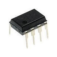
PIC12F1840-I/P Microchip Technology, PIC12F1840-I/P Datasheet - Page 66

PIC12F1840-I/P
Manufacturer Part Number
PIC12F1840-I/P
Description
7 KB Flash, 256 Bytes RAM, 32 MHz Int. Osc, 6 I/0, Enhanced Mid Range Core 8 PDI
Manufacturer
Microchip Technology
Datasheet
1.PIC12F1840-IP.pdf
(382 pages)
Specifications of PIC12F1840-I/P
Processor Series
PIC12F
Core
PIC
Program Memory Type
Flash
Program Memory Size
7 KB
Data Ram Size
256 B
Interface Type
MI2C, SPI, EUSART
Number Of Timers
3
Operating Supply Voltage
1.8 V to 5.5 V
Maximum Operating Temperature
+ 85 C
Mounting Style
Through Hole
Package / Case
PDIP-8
Development Tools By Supplier
MPLAB IDE Software
Minimum Operating Temperature
- 40 C
Lead Free Status / Rohs Status
Lead free / RoHS Compliant
Available stocks
Company
Part Number
Manufacturer
Quantity
Price
Company:
Part Number:
PIC12F1840-I/P
Manufacturer:
MICROCHIP
Quantity:
200
- Current page: 66 of 382
- Download datasheet (4Mb)
PIC12(L)F1840
REGISTER 6-1:
DS41441B-page 66
bit 7
Legend:
R = Readable bit
u = Bit is unchanged
‘1’ = Bit is set
bit 7
bit 6
bit 5
bit 4-3
bit 2-0
Note 1:
CLKREN
R/W-0/0
2:
3:
In this mode, the 25% and 75% duty cycle accuracy will be dependent on the source clock duty cycle.
In this mode, the duty cycle will always be equal to the source clock duty cycle, unless a duty cycle of 0%
is selected.
To route CLKR to pin, CLKOUTEN of Configuration Word 1 = 1 is required. CLKOUTEN of Configuration
Word 1 = 0 will result in F
CLKREN: Reference Clock Module Enable bit
1 = Reference clock module is enabled
0 = Reference clock module is disabled
CLKROE: Reference Clock Output Enable bit
1 = Reference clock output is enabled on CLKR pin
0 = Reference clock output disabled on CLKR pin
CLKRSLR: Reference Clock Slew Rate Control Limiting Enable bit
1 = Slew rate limiting is enabled
0 = Slew rate limiting is disabled
CLKRDC<1:0>: Reference Clock Duty Cycle bits
11 = Clock outputs duty cycle of 75%
10 = Clock outputs duty cycle of 50%
01 = Clock outputs duty cycle of 25%
00 = Clock outputs duty cycle of 0%
CLKRDIV<2:0> Reference Clock Divider bits
111 = Base clock value divided by 128
110 = Base clock value divided by 64
101 = Base clock value divided by 32
100 = Base clock value divided by 16
011 = Base clock value divided by 8
010 = Base clock value divided by 4
001 = Base clock value divided by 2
000 = Base clock value
CLKROE
R/W-0/0
CLKRCON: REFERENCE CLOCK CONTROL REGISTER
W = Writable bit
x = Bit is unknown
‘0’ = Bit is cleared
CLKRSLR
R/W-1/1
OSC
(2)
/4. See
CLKRDC1
R/W-1/1
Section 6.3 “Conflicts with the CLKR pin”
Preliminary
(1)
U = Unimplemented bit, read as ‘0’
-n/n = Value at POR and BOR/Value at all other Resets
CLKRDC0
(3)
R/W-0/0
CLKRDIV2
R/W-0/0
2011 Microchip Technology Inc.
CLKRDIV1
R/W-0/0
for details.
CLKRDIV0
R/W-0/0
bit 0
Related parts for PIC12F1840-I/P
Image
Part Number
Description
Manufacturer
Datasheet
Request
R

Part Number:
Description:
7 KB Flash, 256 Bytes RAM, 32 MHz Int. Osc, 6 I/0, Enhanced Mid Range Core, Nano
Manufacturer:
Microchip Technology
Datasheet:

Part Number:
Description:
MCU, MPU & DSP Development Tools 8 Bit PIC Develop Microcontroller
Manufacturer:
SchmartBoard
Datasheet:

Part Number:
Description:
7 KB Flash, 256 Bytes RAM, 32 MHz Int. Osc, 6 I/0, Enhanced Mid Range Core 8 DFN
Manufacturer:
Microchip Technology

Part Number:
Description:
7 KB Flash, 256 Bytes RAM, 32 MHz Int. Osc, 6 I/0, Enhanced Mid Range Core 8 SOI
Manufacturer:
Microchip Technology

Part Number:
Description:
7 KB Flash, 256 Bytes RAM, 32 MHz Int. Osc, 6 I/0, Enhanced Mid Range Core, Nano
Manufacturer:
Microchip Technology
Datasheet:

Part Number:
Description:
7 KB Flash, 256 Bytes RAM, 32 MHz Int. Osc, 6 I/0, Enhanced Mid Range Core, Nano
Manufacturer:
Microchip Technology
Datasheet:

Part Number:
Description:
7 KB Flash, 256 Bytes RAM, 32 MHz Int. Osc, 6 I/0, Enhanced Mid Range Core, Nano
Manufacturer:
Microchip Technology
Datasheet:

Part Number:
Description:
7 KB Flash, 256 Bytes RAM, 32 MHz Int. Osc, 6 I/0, Enhanced Mid Range Core, Nano
Manufacturer:
Microchip Technology

Part Number:
Description:
7 KB Flash, 256 Bytes RAM, 32 MHz Int. Osc, 6 I/0, Enhanced Mid Range Core, Nano
Manufacturer:
Microchip Technology

Part Number:
Description:
7 KB Flash, 256 Bytes RAM, 32 MHz Int. Osc, 6 I/0, Enhanced Mid Range Core, Nano
Manufacturer:
Microchip Technology
Datasheet:

Part Number:
Description:
7 KB Flash, 256 Bytes RAM, 32 MHz Int. Osc, 6 I/0, Enhanced Mid Range Core, Nano
Manufacturer:
Microchip Technology
Datasheet:

Part Number:
Description:
Manufacturer:
Microchip Technology Inc.
Datasheet:

Part Number:
Description:
Manufacturer:
Microchip Technology Inc.
Datasheet:


