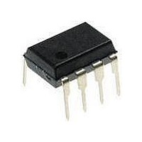
PIC12F1840-I/P Microchip Technology, PIC12F1840-I/P Datasheet - Page 153

PIC12F1840-I/P
Manufacturer Part Number
PIC12F1840-I/P
Description
7 KB Flash, 256 Bytes RAM, 32 MHz Int. Osc, 6 I/0, Enhanced Mid Range Core 8 PDI
Manufacturer
Microchip Technology
Datasheet
1.PIC12F1840-IP.pdf
(382 pages)
Specifications of PIC12F1840-I/P
Processor Series
PIC12F
Core
PIC
Program Memory Type
Flash
Program Memory Size
7 KB
Data Ram Size
256 B
Interface Type
MI2C, SPI, EUSART
Number Of Timers
3
Operating Supply Voltage
1.8 V to 5.5 V
Maximum Operating Temperature
+ 85 C
Mounting Style
Through Hole
Package / Case
PDIP-8
Development Tools By Supplier
MPLAB IDE Software
Minimum Operating Temperature
- 40 C
Lead Free Status / Rohs Status
Lead free / RoHS Compliant
Available stocks
Company
Part Number
Manufacturer
Quantity
Price
Company:
Part Number:
PIC12F1840-I/P
Manufacturer:
MICROCHIP
Quantity:
200
- Current page: 153 of 382
- Download datasheet (4Mb)
19.2
The comparator has 2 control registers: CM1CON0 and
CM1CON1.
The CM1CON0 register (see
Control and Status bits for the following:
• Enable
• Output selection
• Output polarity
• Speed/Power selection
• Hysteresis enable
• Output synchronization
The CM1CON1 register (see
Control bits for the following:
• Interrupt enable
• Interrupt edge polarity
• Positive input channel selection
• Negative input channel selection
19.2.1
Setting the C1ON bit of the CM1CON0 register enables
the comparator for operation. Clearing the C1ON bit
disables the comparator resulting in minimum current
consumption.
19.2.2
The output of the comparator can be monitored by
reading either the C1OUT bit of the CM1CON0 register
or the MC1OUT bit of the CMOUT register. In order to
make the output available for an external connection,
the following conditions must be true:
• C1OE bit of the CM1CON0 register must be set
• Corresponding TRIS bit must be cleared
• C1ON bit of the CM1CON0 register must be set
2011 Microchip Technology Inc.
Note 1: The C1OE bit of the CM1CON0 register
2: The internal output of the comparator is
Comparator Control
COMPARATOR ENABLE
COMPARATOR OUTPUT
SELECTION
overrides the PORT data latch. Setting
the C1ON bit of the CM1CON0 register
has no impact on the port override.
latched with each instruction cycle.
Unless otherwise specified, external
outputs are not latched.
Register
Register
19-1) contains
19-2) contains
Preliminary
19.2.3
Inverting the output of the comparator is functionally
equivalent to swapping the comparator inputs. The
polarity of the comparator output can be inverted by
setting the C1POL bit of the CM1CON0 register.
Clearing the C1POL bit results in a non-inverted output.
Table 19-1
conditions, including polarity control.
TABLE 19-1:
19.2.4
The trade-off between speed or power can be opti-
mized during program execution with the C1SP control
bit. The default state for this bit is ‘1’ which selects the
normal speed mode. Device power consumption can
be optimized at the cost of slower comparator propaga-
tion delay by clearing the C1SP bit to ‘0’.
Input Condition
C1V
C1V
C1V
C1V
N
N
N
N
> C1V
< C1V
> C1V
< C1V
COMPARATOR OUTPUT POLARITY
COMPARATOR SPEED/POWER
SELECTION
shows the output state versus input
PIC12(L)F1840
P
P
P
P
COMPARATOR OUTPUT
STATE VS. INPUT
CONDITIONS
C1POL
0
0
1
1
DS41441B-page 153
C1OUT
0
1
1
0
Related parts for PIC12F1840-I/P
Image
Part Number
Description
Manufacturer
Datasheet
Request
R

Part Number:
Description:
7 KB Flash, 256 Bytes RAM, 32 MHz Int. Osc, 6 I/0, Enhanced Mid Range Core, Nano
Manufacturer:
Microchip Technology
Datasheet:

Part Number:
Description:
MCU, MPU & DSP Development Tools 8 Bit PIC Develop Microcontroller
Manufacturer:
SchmartBoard
Datasheet:

Part Number:
Description:
7 KB Flash, 256 Bytes RAM, 32 MHz Int. Osc, 6 I/0, Enhanced Mid Range Core 8 DFN
Manufacturer:
Microchip Technology

Part Number:
Description:
7 KB Flash, 256 Bytes RAM, 32 MHz Int. Osc, 6 I/0, Enhanced Mid Range Core 8 SOI
Manufacturer:
Microchip Technology

Part Number:
Description:
7 KB Flash, 256 Bytes RAM, 32 MHz Int. Osc, 6 I/0, Enhanced Mid Range Core, Nano
Manufacturer:
Microchip Technology
Datasheet:

Part Number:
Description:
7 KB Flash, 256 Bytes RAM, 32 MHz Int. Osc, 6 I/0, Enhanced Mid Range Core, Nano
Manufacturer:
Microchip Technology
Datasheet:

Part Number:
Description:
7 KB Flash, 256 Bytes RAM, 32 MHz Int. Osc, 6 I/0, Enhanced Mid Range Core, Nano
Manufacturer:
Microchip Technology
Datasheet:

Part Number:
Description:
7 KB Flash, 256 Bytes RAM, 32 MHz Int. Osc, 6 I/0, Enhanced Mid Range Core, Nano
Manufacturer:
Microchip Technology

Part Number:
Description:
7 KB Flash, 256 Bytes RAM, 32 MHz Int. Osc, 6 I/0, Enhanced Mid Range Core, Nano
Manufacturer:
Microchip Technology

Part Number:
Description:
7 KB Flash, 256 Bytes RAM, 32 MHz Int. Osc, 6 I/0, Enhanced Mid Range Core, Nano
Manufacturer:
Microchip Technology
Datasheet:

Part Number:
Description:
7 KB Flash, 256 Bytes RAM, 32 MHz Int. Osc, 6 I/0, Enhanced Mid Range Core, Nano
Manufacturer:
Microchip Technology
Datasheet:

Part Number:
Description:
Manufacturer:
Microchip Technology Inc.
Datasheet:

Part Number:
Description:
Manufacturer:
Microchip Technology Inc.
Datasheet:


