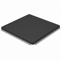
LPC2468FBD208,551 NXP Semiconductors, LPC2468FBD208,551 Datasheet - Page 22

LPC2468FBD208,551
Manufacturer Part Number
LPC2468FBD208,551
Description
IC ARM7 MCU FLASH 512K 208-LQFP
Manufacturer
NXP Semiconductors
Series
LPC2400r
Specifications of LPC2468FBD208,551
Program Memory Type
FLASH
Program Memory Size
512KB (512K x 8)
Package / Case
208-LQFP
Core Processor
ARM7
Core Size
16/32-Bit
Speed
72MHz
Connectivity
CAN, EBI/EMI, Ethernet, I²C, Microwire, MMC, SPI, SSI, SSP, UART/USART, USB OTG
Peripherals
Brown-out Detect/Reset, DMA, I²S, POR, PWM, WDT
Number Of I /o
160
Ram Size
98K x 8
Voltage - Supply (vcc/vdd)
3 V ~ 3.6 V
Data Converters
A/D 8x10b; D/A 1x10b
Oscillator Type
Internal
Operating Temperature
-40°C ~ 85°C
Processor Series
LPC24
Core
ARM7TDMI-S
Data Bus Width
16 bit, 32 bit
Data Ram Size
98 KB
Interface Type
CAN/I2S/ISP/SSP/UART/USB
Maximum Clock Frequency
72 MHz
Number Of Programmable I/os
160
Number Of Timers
6
Operating Supply Voltage
3.3 V
Maximum Operating Temperature
+ 85 C
Mounting Style
SMD/SMT
3rd Party Development Tools
MDK-ARM, RL-ARM, ULINK2, IRD-LPC2468-DEV, SAB-TFBGA208, KSK-LPC2468-PL
Development Tools By Supplier
OM10100
Minimum Operating Temperature
- 40 C
On-chip Adc
8-ch x 10-bit
On-chip Dac
1-ch x 10-bit
Lead Free Status / RoHS Status
Lead free / RoHS Compliant
For Use With
622-1025 - KIT DEV IND REF DESIGN LPC2468622-1024 - BOARD SCKT ADAPTER FOR TFBGA208568-4358 - DISPLAY QVGA TFT FOR OM10100568-4309 - BOARD EXTENSION LPCSTICK568-4308 - EVAL LPC-STICK WITH LPC2468MCB2400U - BOARD EVAL MCB2400 + ULINK2MCB2400 - BOARD EVAL FOR NXP LPC246X SER622-1005 - USB IN-CIRCUIT PROG ARM7 LPC2K
Eeprom Size
-
Lead Free Status / Rohs Status
Lead free / RoHS Compliant
Other names
568-4261
935282457551
LPC2468FBD208-S
935282457551
LPC2468FBD208-S
Available stocks
Company
Part Number
Manufacturer
Quantity
Price
Company:
Part Number:
LPC2468FBD208,551
Manufacturer:
TI
Quantity:
1 908
Company:
Part Number:
LPC2468FBD208,551
Manufacturer:
NXP Semiconductors
Quantity:
10 000
- Current page: 22 of 792
- Download datasheet (5Mb)
NXP Semiconductors
5. LPC2400 memory re-mapping and boot ROM
UM10237_4
User manual
5.1 Memory map concepts and operating modes
The basic concept on the LPC2400 is that each memory area has a "natural" location in
the memory map. This is the address range for which code residing in that area is written.
The bulk of each memory space remains permanently fixed in the same location,
eliminating the need to have portions of the code designed to run in different address
ranges.
Because of the location of the interrupt vectors on the ARM7 processor (at addresses
0x0000 0000 through 0x0000 001C, as shown in
Boot ROM and SRAM spaces need to be re-mapped in order to allow alternative uses of
interrupts in the different operating modes described in
interrupts is accomplished via the Memory Mapping Control feature
mapping control” on page
Table 18.
Address
0x0000 0000
0x0000 0004
0x0000 0008
0x0000 000C
0x0000 0010
0x0000 0014
0x0000 0018
0x0000 001C
ARM exception vector locations
Exception
Reset
Undefined Instruction
Software Interrupt
Prefetch Abort (instruction fetch memory fault)
Data Abort (data access memory fault)
Reserved
Note: Identified as reserved in ARM documentation, this location is used
by the Boot Loader as the Valid User Program key when booting from
on-chip flash memory. This is described in detail in
IRQ
FIQ
Rev. 04 — 26 August 2009
24).
Chapter 2: LPC24XX Memory mapping
Table 2–18
Table
below), a small portion of the
2–19. Re-mapping of the
(Section 2–6 “Memory
Section
UM10237
© NXP B.V. 2009. All rights reserved.
30–5.1.1.
22 of 792
Related parts for LPC2468FBD208,551
Image
Part Number
Description
Manufacturer
Datasheet
Request
R
Part Number:
Description:
NXP Semiconductors designed the LPC2468 microcontroller around a 16-bit/32-bitARM7TDMI-S CPU core with real-time debug interfaces that include both JTAG andembedded trace
Manufacturer:
NXP Semiconductors
Datasheet:

Part Number:
Description:
MCU, MPU & DSP Development Tools Ind. Ref. Design LPC2468 Dev Kit V1.2
Manufacturer:
FDI
Datasheet:

Part Number:
Description:
MCU, MPU & DSP Development Tools KICKSTART KIT NXP LPC2468
Manufacturer:
IAR Systems

Part Number:
Description:
MCU, MPU & DSP Development Tools DEV BRD FOR LPC2468 128MBFLASH 16MBSDRAM
Manufacturer:
Olimex Ltd.
Datasheet:

Part Number:
Description:
MCU, MPU & DSP Development Tools LPC2468 OEM BRD OEM BASE BRD BUNDLE
Manufacturer:
Embedded Artists
Part Number:
Description:
Lpc2468 Single-chip 16-bit/32-bit Micro; 512 Kb Flash, Ethernet, Can, Isp/iap, Usb 2.0 Device/host/otg, External Memory Interface
Manufacturer:
NXP Semiconductors
Datasheet:
Part Number:
Description:
NXP Semiconductors designed the LPC2420/2460 microcontroller around a 16-bit/32-bitARM7TDMI-S CPU core with real-time debug interfaces that include both JTAG andembedded trace
Manufacturer:
NXP Semiconductors
Datasheet:

Part Number:
Description:
NXP Semiconductors designed the LPC2458 microcontroller around a 16-bit/32-bitARM7TDMI-S CPU core with real-time debug interfaces that include both JTAG andembedded trace
Manufacturer:
NXP Semiconductors
Datasheet:
Part Number:
Description:
NXP Semiconductors designed the LPC2470 microcontroller, powered by theARM7TDMI-S core, to be a highly integrated microcontroller for a wide range ofapplications that require advanced communications and high quality graphic displays
Manufacturer:
NXP Semiconductors
Datasheet:
Part Number:
Description:
NXP Semiconductors designed the LPC2478 microcontroller, powered by theARM7TDMI-S core, to be a highly integrated microcontroller for a wide range ofapplications that require advanced communications and high quality graphic displays
Manufacturer:
NXP Semiconductors
Datasheet:
Part Number:
Description:
The Philips Semiconductors XA (eXtended Architecture) family of 16-bit single-chip microcontrollers is powerful enough to easily handle the requirements of high performance embedded applications, yet inexpensive enough to compete in the market for hi
Manufacturer:
NXP Semiconductors
Datasheet:
Part Number:
Description:
The XA-S3 device is a member of Philips Semiconductors? XA(eXtended Architecture) family of high performance 16-bitsingle-chip microcontrollers
Manufacturer:
NXP Semiconductors
Datasheet:

Part Number:
Description:
The NXP BlueStreak LH75401/LH75411 family consists of two low-cost 16/32-bit System-on-Chip (SoC) devices
Manufacturer:
NXP Semiconductors
Datasheet:

Part Number:
Description:
The NXP LPC3130/3131 combine an 180 MHz ARM926EJ-S CPU core, high-speed USB2
Manufacturer:
NXP Semiconductors
Datasheet:


