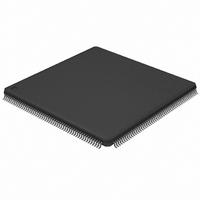
LPC2468FBD208,551 NXP Semiconductors, LPC2468FBD208,551 Datasheet - Page 613

LPC2468FBD208,551
Manufacturer Part Number
LPC2468FBD208,551
Description
IC ARM7 MCU FLASH 512K 208-LQFP
Manufacturer
NXP Semiconductors
Series
LPC2400r
Specifications of LPC2468FBD208,551
Program Memory Type
FLASH
Program Memory Size
512KB (512K x 8)
Package / Case
208-LQFP
Core Processor
ARM7
Core Size
16/32-Bit
Speed
72MHz
Connectivity
CAN, EBI/EMI, Ethernet, I²C, Microwire, MMC, SPI, SSI, SSP, UART/USART, USB OTG
Peripherals
Brown-out Detect/Reset, DMA, I²S, POR, PWM, WDT
Number Of I /o
160
Ram Size
98K x 8
Voltage - Supply (vcc/vdd)
3 V ~ 3.6 V
Data Converters
A/D 8x10b; D/A 1x10b
Oscillator Type
Internal
Operating Temperature
-40°C ~ 85°C
Processor Series
LPC24
Core
ARM7TDMI-S
Data Bus Width
16 bit, 32 bit
Data Ram Size
98 KB
Interface Type
CAN/I2S/ISP/SSP/UART/USB
Maximum Clock Frequency
72 MHz
Number Of Programmable I/os
160
Number Of Timers
6
Operating Supply Voltage
3.3 V
Maximum Operating Temperature
+ 85 C
Mounting Style
SMD/SMT
3rd Party Development Tools
MDK-ARM, RL-ARM, ULINK2, IRD-LPC2468-DEV, SAB-TFBGA208, KSK-LPC2468-PL
Development Tools By Supplier
OM10100
Minimum Operating Temperature
- 40 C
On-chip Adc
8-ch x 10-bit
On-chip Dac
1-ch x 10-bit
Lead Free Status / RoHS Status
Lead free / RoHS Compliant
For Use With
622-1025 - KIT DEV IND REF DESIGN LPC2468622-1024 - BOARD SCKT ADAPTER FOR TFBGA208568-4358 - DISPLAY QVGA TFT FOR OM10100568-4309 - BOARD EXTENSION LPCSTICK568-4308 - EVAL LPC-STICK WITH LPC2468MCB2400U - BOARD EVAL MCB2400 + ULINK2MCB2400 - BOARD EVAL FOR NXP LPC246X SER622-1005 - USB IN-CIRCUIT PROG ARM7 LPC2K
Eeprom Size
-
Lead Free Status / Rohs Status
Lead free / RoHS Compliant
Other names
568-4261
935282457551
LPC2468FBD208-S
935282457551
LPC2468FBD208-S
Available stocks
Company
Part Number
Manufacturer
Quantity
Price
Company:
Part Number:
LPC2468FBD208,551
Manufacturer:
TI
Quantity:
1 908
Company:
Part Number:
LPC2468FBD208,551
Manufacturer:
NXP Semiconductors
Quantity:
10 000
- Current page: 613 of 792
- Download datasheet (5Mb)
NXP Semiconductors
5. Register description
UM10237_4
User manual
Fig 127. Simple I
TRANSMITTER
(MASTER)
2
S configurations and bus timing
SCK
WS
SD
SCK: serial clock
WS: word select
SD: serial data
Table 23–531
their functions. Following the table are details for each register.
Table 531. Summary of I
Name
I2SDAO
I2SDAI
I2STXFIFO
I2SRXFIFO
I2SSTATE
I2SDMA1
I2SDMA2
right channel
word n-1
TRANSMITTER
Description
Digital Audio Output Register. Contains control
bits for the I
Digital Audio Input Register. Contains control
bits for the I
Transmit FIFO. Access register for the 8
transmitter FIFO.
Receive FIFO. Access register for the 8
receiver FIFO.
Status Feedback Register. Contains status
information about the I
DMA Configuration Register 1. Contains control
information for DMA request 1.
DMA Configuration Register 2. Contains control
information for DMA request 2.
shows the registers associated with the I
RECEIVER
(SLAVE)
(SLAVE)
MSB
Rev. 04 — 26 August 2009
2
2
2
S registers
S transmit channel.
S receive channel.
CONTROLLER
(MASTER)
SCK
WS
SD
2
S interface.
left channel
word n
RECEIVER
TRANSMITTER
(SLAVE)
(SLAVE)
×
×
32 bit
32 bit
Chapter 23: LPC24XX I
LSB
2
S interface and a summary of
SCK: serial clock
WS: word select
SD: serial data
Access Reset
R/W
R/W
WO
RO
RO
R/W
R/W
MSB
right channel
word n+1
Value
UM10237
© NXP B.V. 2009. All rights reserved.
RECEIVER
[1]
(MASTER)
Address
0xE008 8000
0xE008 8004
0xE008 8008
0xE008 800C
0xE008 8010
0xE008 8014
0xE008 8018
2
S interface
613 of 792
Related parts for LPC2468FBD208,551
Image
Part Number
Description
Manufacturer
Datasheet
Request
R
Part Number:
Description:
NXP Semiconductors designed the LPC2468 microcontroller around a 16-bit/32-bitARM7TDMI-S CPU core with real-time debug interfaces that include both JTAG andembedded trace
Manufacturer:
NXP Semiconductors
Datasheet:

Part Number:
Description:
MCU, MPU & DSP Development Tools Ind. Ref. Design LPC2468 Dev Kit V1.2
Manufacturer:
FDI
Datasheet:

Part Number:
Description:
MCU, MPU & DSP Development Tools KICKSTART KIT NXP LPC2468
Manufacturer:
IAR Systems

Part Number:
Description:
MCU, MPU & DSP Development Tools DEV BRD FOR LPC2468 128MBFLASH 16MBSDRAM
Manufacturer:
Olimex Ltd.
Datasheet:

Part Number:
Description:
MCU, MPU & DSP Development Tools LPC2468 OEM BRD OEM BASE BRD BUNDLE
Manufacturer:
Embedded Artists
Part Number:
Description:
Lpc2468 Single-chip 16-bit/32-bit Micro; 512 Kb Flash, Ethernet, Can, Isp/iap, Usb 2.0 Device/host/otg, External Memory Interface
Manufacturer:
NXP Semiconductors
Datasheet:
Part Number:
Description:
NXP Semiconductors designed the LPC2420/2460 microcontroller around a 16-bit/32-bitARM7TDMI-S CPU core with real-time debug interfaces that include both JTAG andembedded trace
Manufacturer:
NXP Semiconductors
Datasheet:

Part Number:
Description:
NXP Semiconductors designed the LPC2458 microcontroller around a 16-bit/32-bitARM7TDMI-S CPU core with real-time debug interfaces that include both JTAG andembedded trace
Manufacturer:
NXP Semiconductors
Datasheet:
Part Number:
Description:
NXP Semiconductors designed the LPC2470 microcontroller, powered by theARM7TDMI-S core, to be a highly integrated microcontroller for a wide range ofapplications that require advanced communications and high quality graphic displays
Manufacturer:
NXP Semiconductors
Datasheet:
Part Number:
Description:
NXP Semiconductors designed the LPC2478 microcontroller, powered by theARM7TDMI-S core, to be a highly integrated microcontroller for a wide range ofapplications that require advanced communications and high quality graphic displays
Manufacturer:
NXP Semiconductors
Datasheet:
Part Number:
Description:
The Philips Semiconductors XA (eXtended Architecture) family of 16-bit single-chip microcontrollers is powerful enough to easily handle the requirements of high performance embedded applications, yet inexpensive enough to compete in the market for hi
Manufacturer:
NXP Semiconductors
Datasheet:
Part Number:
Description:
The XA-S3 device is a member of Philips Semiconductors? XA(eXtended Architecture) family of high performance 16-bitsingle-chip microcontrollers
Manufacturer:
NXP Semiconductors
Datasheet:

Part Number:
Description:
The NXP BlueStreak LH75401/LH75411 family consists of two low-cost 16/32-bit System-on-Chip (SoC) devices
Manufacturer:
NXP Semiconductors
Datasheet:

Part Number:
Description:
The NXP LPC3130/3131 combine an 180 MHz ARM926EJ-S CPU core, high-speed USB2
Manufacturer:
NXP Semiconductors
Datasheet:


