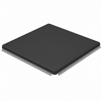
LPC2468FBD208,551 NXP Semiconductors, LPC2468FBD208,551 Datasheet - Page 675

LPC2468FBD208,551
Manufacturer Part Number
LPC2468FBD208,551
Description
IC ARM7 MCU FLASH 512K 208-LQFP
Manufacturer
NXP Semiconductors
Series
LPC2400r
Specifications of LPC2468FBD208,551
Program Memory Type
FLASH
Program Memory Size
512KB (512K x 8)
Package / Case
208-LQFP
Core Processor
ARM7
Core Size
16/32-Bit
Speed
72MHz
Connectivity
CAN, EBI/EMI, Ethernet, I²C, Microwire, MMC, SPI, SSI, SSP, UART/USART, USB OTG
Peripherals
Brown-out Detect/Reset, DMA, I²S, POR, PWM, WDT
Number Of I /o
160
Ram Size
98K x 8
Voltage - Supply (vcc/vdd)
3 V ~ 3.6 V
Data Converters
A/D 8x10b; D/A 1x10b
Oscillator Type
Internal
Operating Temperature
-40°C ~ 85°C
Processor Series
LPC24
Core
ARM7TDMI-S
Data Bus Width
16 bit, 32 bit
Data Ram Size
98 KB
Interface Type
CAN/I2S/ISP/SSP/UART/USB
Maximum Clock Frequency
72 MHz
Number Of Programmable I/os
160
Number Of Timers
6
Operating Supply Voltage
3.3 V
Maximum Operating Temperature
+ 85 C
Mounting Style
SMD/SMT
3rd Party Development Tools
MDK-ARM, RL-ARM, ULINK2, IRD-LPC2468-DEV, SAB-TFBGA208, KSK-LPC2468-PL
Development Tools By Supplier
OM10100
Minimum Operating Temperature
- 40 C
On-chip Adc
8-ch x 10-bit
On-chip Dac
1-ch x 10-bit
Lead Free Status / RoHS Status
Lead free / RoHS Compliant
For Use With
622-1025 - KIT DEV IND REF DESIGN LPC2468622-1024 - BOARD SCKT ADAPTER FOR TFBGA208568-4358 - DISPLAY QVGA TFT FOR OM10100568-4309 - BOARD EXTENSION LPCSTICK568-4308 - EVAL LPC-STICK WITH LPC2468MCB2400U - BOARD EVAL MCB2400 + ULINK2MCB2400 - BOARD EVAL FOR NXP LPC246X SER622-1005 - USB IN-CIRCUIT PROG ARM7 LPC2K
Eeprom Size
-
Lead Free Status / Rohs Status
Lead free / RoHS Compliant
Other names
568-4261
935282457551
LPC2468FBD208-S
935282457551
LPC2468FBD208-S
Available stocks
Company
Part Number
Manufacturer
Quantity
Price
Company:
Part Number:
LPC2468FBD208,551
Manufacturer:
TI
Quantity:
1 908
Company:
Part Number:
LPC2468FBD208,551
Manufacturer:
NXP Semiconductors
Quantity:
10 000
- Current page: 675 of 792
- Download datasheet (5Mb)
NXP Semiconductors
5. Operation
UM10237_4
User manual
Table 599: D/A Converter Register (DACR - address 0xE006 C000) bit description
Bits 21:20 of the PINSEL1 register
(PINSEL1 - 0xE002 C004)” on page
controlling the state of pin P0.26/AD0.3/AOUT/RXD3. When these bits are 10, the DAC is
powered on and active.
The settling times noted in the description of the BIAS bit are valid for a capacitance load
on the AOUT pin not exceeding 100 pF. A load impedance value greater than that value
will cause settling time longer than the specified time. One or more graph(s) of load
impedance vs. settling time will be included in the final data sheet.
Bit
5:0
15:6
16
31:17 -
Symbol Value
-
VALUE
BIAS
0
1
Rev. 04 — 26 August 2009
Description
Reserved, user software should not write ones to reserved
bits. The value read from a reserved bit is not defined.
After the selected settling time after this field is written with a
new VALUE, the voltage on the A
is VALUE/1024 × VREF.
The settling time of the DAC is 1 μ s max, and the maximum
current is 700 μ A.
The settling time of the DAC is 2.5 μ s and the maximum
current is 350 μ A.
Reserved, user software should not write ones to reserved
bits. The value read from a reserved bit is not defined.
Chapter 29: LPC24XX Digital-to Analog Converter (DAC)
(Section 9–5.2 “Pin Function Select Register 1
180) control whether the DAC is enabled and
OUT
pin (with respect to V
UM10237
© NXP B.V. 2009. All rights reserved.
SSA
)
675 of 792
Reset
Value
NA
0
0
NA
Related parts for LPC2468FBD208,551
Image
Part Number
Description
Manufacturer
Datasheet
Request
R
Part Number:
Description:
NXP Semiconductors designed the LPC2468 microcontroller around a 16-bit/32-bitARM7TDMI-S CPU core with real-time debug interfaces that include both JTAG andembedded trace
Manufacturer:
NXP Semiconductors
Datasheet:

Part Number:
Description:
MCU, MPU & DSP Development Tools Ind. Ref. Design LPC2468 Dev Kit V1.2
Manufacturer:
FDI
Datasheet:

Part Number:
Description:
MCU, MPU & DSP Development Tools KICKSTART KIT NXP LPC2468
Manufacturer:
IAR Systems

Part Number:
Description:
MCU, MPU & DSP Development Tools DEV BRD FOR LPC2468 128MBFLASH 16MBSDRAM
Manufacturer:
Olimex Ltd.
Datasheet:

Part Number:
Description:
MCU, MPU & DSP Development Tools LPC2468 OEM BRD OEM BASE BRD BUNDLE
Manufacturer:
Embedded Artists
Part Number:
Description:
Lpc2468 Single-chip 16-bit/32-bit Micro; 512 Kb Flash, Ethernet, Can, Isp/iap, Usb 2.0 Device/host/otg, External Memory Interface
Manufacturer:
NXP Semiconductors
Datasheet:
Part Number:
Description:
NXP Semiconductors designed the LPC2420/2460 microcontroller around a 16-bit/32-bitARM7TDMI-S CPU core with real-time debug interfaces that include both JTAG andembedded trace
Manufacturer:
NXP Semiconductors
Datasheet:

Part Number:
Description:
NXP Semiconductors designed the LPC2458 microcontroller around a 16-bit/32-bitARM7TDMI-S CPU core with real-time debug interfaces that include both JTAG andembedded trace
Manufacturer:
NXP Semiconductors
Datasheet:
Part Number:
Description:
NXP Semiconductors designed the LPC2470 microcontroller, powered by theARM7TDMI-S core, to be a highly integrated microcontroller for a wide range ofapplications that require advanced communications and high quality graphic displays
Manufacturer:
NXP Semiconductors
Datasheet:
Part Number:
Description:
NXP Semiconductors designed the LPC2478 microcontroller, powered by theARM7TDMI-S core, to be a highly integrated microcontroller for a wide range ofapplications that require advanced communications and high quality graphic displays
Manufacturer:
NXP Semiconductors
Datasheet:
Part Number:
Description:
The Philips Semiconductors XA (eXtended Architecture) family of 16-bit single-chip microcontrollers is powerful enough to easily handle the requirements of high performance embedded applications, yet inexpensive enough to compete in the market for hi
Manufacturer:
NXP Semiconductors
Datasheet:
Part Number:
Description:
The XA-S3 device is a member of Philips Semiconductors? XA(eXtended Architecture) family of high performance 16-bitsingle-chip microcontrollers
Manufacturer:
NXP Semiconductors
Datasheet:

Part Number:
Description:
The NXP BlueStreak LH75401/LH75411 family consists of two low-cost 16/32-bit System-on-Chip (SoC) devices
Manufacturer:
NXP Semiconductors
Datasheet:

Part Number:
Description:
The NXP LPC3130/3131 combine an 180 MHz ARM926EJ-S CPU core, high-speed USB2
Manufacturer:
NXP Semiconductors
Datasheet:


