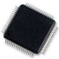
UPD78F0890GK(A)-GAJ-AX NEC, UPD78F0890GK(A)-GAJ-AX Datasheet - Page 230

UPD78F0890GK(A)-GAJ-AX
Manufacturer Part Number
UPD78F0890GK(A)-GAJ-AX
Description
8BIT MCU, 128K FLASH, 7K RAM, LQFP
Manufacturer
NEC
Datasheet
1.UPD78F0890GKA-GAJ-AX.pdf
(732 pages)
Specifications of UPD78F0890GK(A)-GAJ-AX
Controller Family/series
UPD78F
No. Of I/o's
55
Ram Memory Size
7KB
Cpu Speed
20MHz
No. Of Timers
10
No. Of Pwm
RoHS Compliant
Core Size
8bit
Program Memory Size
128KB
Oscillator Type
External, Internal
- Current page: 230 of 732
- Download datasheet (4Mb)
(3) Port mode registers 1 and 3 (PM1, PM3)
230
These registers set port 1 and 3 input/output in 1-bit units.
When using the P17/TO50/TI50 and P33/TO51/TI51/INTP4 pins for timer output, clear PM17 and PM33 and the
output latches of P17 and P33 to 0.
When using the P17/TO50/TI50 and P33/TO51/TI51/INTP4 pins for timer input, set PM17 and PM33 to 1. The
output latches of P17 and P33 at this time may be 0 or 1.
PM1 and PM3 can be set by a 1-bit or 8-bit memory manipulation instruction.
Reset signal generation sets these registers to FFH.
Address: FF21H
Symbol
PM1
Address: FF23H
Symbol
PM3
PM1n
PM3n
PM17
7
0
1
7
1
0
1
After reset: FFH
After reset: FFH
Output mode (output buffer on)
Input mode (output buffer off)
Output mode (output buffer on)
Input mode (output buffer off)
PM16
CHAPTER 8 8-BIT TIMER/EVENT COUNTERS 50 AND 51
6
6
1
Figure 8-10. Format of Port Mode Register 3 (PM3)
Figure 8-9. Format of Port Mode Register 1 (PM1)
PM15
5
5
1
R/W
R/W
P1n pin I/O mode selection (n = 0 to 7)
P3n pin I/O mode selection (n = 0 to 3)
User’s Manual U17554EJ4V0UD
PM14
4
4
1
PM13
PM33
3
3
PM12
PM32
2
2
PM11
PM31
1
1
PM10
PM30
0
0
Related parts for UPD78F0890GK(A)-GAJ-AX
Image
Part Number
Description
Manufacturer
Datasheet
Request
R

Part Number:
Description:
16/8 bit single-chip microcomputer
Manufacturer:
NEC
Datasheet:

Part Number:
Description:
Dual audio power amp circuit
Manufacturer:
NEC
Datasheet:

Part Number:
Description:
Dual comparator
Manufacturer:
NEC
Datasheet:

Part Number:
Description:
MOS type composite field effect transistor
Manufacturer:
NEC
Datasheet:

Part Number:
Description:
50 V/100 mA FET array incorporating 2 N-ch MOSFETs
Manufacturer:
NEC
Datasheet:

Part Number:
Description:
6-pin small MM high-frequency double transistor
Manufacturer:
NEC
Datasheet:

Part Number:
Description:
6-pin small MM high-frequency double transistor
Manufacturer:
NEC
Datasheet:

Part Number:
Description:
6-pin small MM high-frequency double transistor
Manufacturer:
NEC
Datasheet:

Part Number:
Description:
6-pin small MM high-frequency double transistor
Manufacturer:
NEC
Datasheet:

Part Number:
Description:
Twin transistors equipped with different model chips(6P small MM)
Manufacturer:
NEC
Datasheet:

Part Number:
Description:
Bipolar analog integrated circuit
Manufacturer:
NEC
Datasheet:


