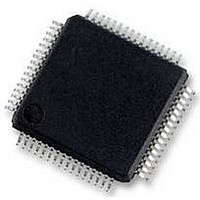
UPD78F0890GK(A)-GAJ-AX NEC, UPD78F0890GK(A)-GAJ-AX Datasheet - Page 35

UPD78F0890GK(A)-GAJ-AX
Manufacturer Part Number
UPD78F0890GK(A)-GAJ-AX
Description
8BIT MCU, 128K FLASH, 7K RAM, LQFP
Manufacturer
NEC
Datasheet
1.UPD78F0890GKA-GAJ-AX.pdf
(732 pages)
Specifications of UPD78F0890GK(A)-GAJ-AX
Controller Family/series
UPD78F
No. Of I/o's
55
Ram Memory Size
7KB
Cpu Speed
20MHz
No. Of Timers
10
No. Of Pwm
RoHS Compliant
Core Size
8bit
Program Memory Size
128KB
Oscillator Type
External, Internal
- Current page: 35 of 732
- Download datasheet (4Mb)
2.2.11 P130 to P132 (port 13)
pins for timer I/O. The following operation modes can be specified in 1-bit units.
(1)
of an on-chip pull-up resistor can be specified by pull-up resistor option register 13 (PU13).
(2) Control mode
P130 functions as a 1-bit output-only port. P131 and P132 function as a 2-bit I/O port. These pins also function as
P131 and P132 can be set to input or output in 1 bit units using port mode register 13 (PM13). P131 and P132 use
(b) EXLVI
(c) X1, X2
(d) EXCLK
(e) XT1, XT2
(f) EXCLKS
P130, P131 and P132 function as timer I/O and serial interface chip select input.
(a) TI003
(b) TI013
(c) TO03
Port mode
This is a potential input pin for external low-voltage detection.
These are the pins for connecting a resonator for high-speed system clock.
When supplying an external clock, input a signal to the X1 pin and input the inverse signal to the X2 pin.
This is an external clock input pin for main system clock.
These are the pins for connecting a resonator for subsystem clock.
When supplying an external clock, input a signal to the XT1 pin and input the inverse signal to the XT2 pin.
This is an external clock input pin for subsystem clock.
This is the pin for inputting an external count clock to 16-bit timer/event counter 03 and is also for inputting a
capture trigger signal to the capture registers (CR003, CR013) of 16-bit timer/event counter 03.
This is the pin for inputting a capture trigger signal to the capture register (CR003) of 16-bit timer/event
counter 03.
This is a timer output pin.
Caution Connect P121/X1 as follows when writing the flash memory with a flash programmer.
Remark The X1 and X2 pins can be used as on-chip debug mode setting pins when the on-chip debug
The above connection is not necessary when writing the flash memory by means of self
programming.
function is used. For details, refer to CHAPTER 25 ON-CHIP DEBUG FUNCTION.
- P121/X1: When using this pin as a port, connect it to V
recommended) (in the input mode) or leave it open (in the output mode).
CHAPTER 2 PIN FUNCTIONS
User’s Manual U17554EJ4V0UD
SS
via a resistor (10 kΩ:
35
Related parts for UPD78F0890GK(A)-GAJ-AX
Image
Part Number
Description
Manufacturer
Datasheet
Request
R

Part Number:
Description:
16/8 bit single-chip microcomputer
Manufacturer:
NEC
Datasheet:

Part Number:
Description:
Dual audio power amp circuit
Manufacturer:
NEC
Datasheet:

Part Number:
Description:
Dual comparator
Manufacturer:
NEC
Datasheet:

Part Number:
Description:
MOS type composite field effect transistor
Manufacturer:
NEC
Datasheet:

Part Number:
Description:
50 V/100 mA FET array incorporating 2 N-ch MOSFETs
Manufacturer:
NEC
Datasheet:

Part Number:
Description:
6-pin small MM high-frequency double transistor
Manufacturer:
NEC
Datasheet:

Part Number:
Description:
6-pin small MM high-frequency double transistor
Manufacturer:
NEC
Datasheet:

Part Number:
Description:
6-pin small MM high-frequency double transistor
Manufacturer:
NEC
Datasheet:

Part Number:
Description:
6-pin small MM high-frequency double transistor
Manufacturer:
NEC
Datasheet:

Part Number:
Description:
Twin transistors equipped with different model chips(6P small MM)
Manufacturer:
NEC
Datasheet:

Part Number:
Description:
Bipolar analog integrated circuit
Manufacturer:
NEC
Datasheet:


