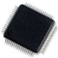
UPD78F0890GK(A)-GAJ-AX NEC, UPD78F0890GK(A)-GAJ-AX Datasheet - Page 95

UPD78F0890GK(A)-GAJ-AX
Manufacturer Part Number
UPD78F0890GK(A)-GAJ-AX
Description
8BIT MCU, 128K FLASH, 7K RAM, LQFP
Manufacturer
NEC
Datasheet
1.UPD78F0890GKA-GAJ-AX.pdf
(732 pages)
Specifications of UPD78F0890GK(A)-GAJ-AX
Controller Family/series
UPD78F
No. Of I/o's
55
Ram Memory Size
7KB
Cpu Speed
20MHz
No. Of Timers
10
No. Of Pwm
RoHS Compliant
Core Size
8bit
Program Memory Size
128KB
Oscillator Type
External, Internal
- Current page: 95 of 732
- Download datasheet (4Mb)
5.2.2 Port 1
using port mode register 1 (PM1). When the P10 to P17 pins are used as an input port, use of an on-chip pull-up
resistor can be specified in 1-bit units by pull-up resistor option register 1 (PU1).
Port 1 is an 8-bit I/O port with an output latch. Port 1 can be set to the input mode or output mode in 1-bit units
This port can also be used for external interrupt request input, serial interface data I/O, clock I/O, and timer I/O.
Reset signal generation sets port 1 to input mode.
Figures 5-4 to 5-6 show block diagrams of port 1.
Caution To use P10/SCK10/TxD61 and P12/SO10 as general-purpose ports, set serial operation mode
WR
WR
WR
P1:
PU1:
PM1:
RD:
WR××: Write signal
RD
PORT
PU
PM
register 10 (CSIM10) and serial clock selection register 10 (CSIC10) to the default status (00H).
Read signal
Port register 1
Pull-up resistor option register 1
Port mode register 1
(P10, P16, P17)
PM10, PM16,
PU10, PU16,
Output latch
Alternate
Alternate
function
function
PM17
PU17
PM1
PU1
P1
Figure 5-4. Block Diagram of P10, P16 and P17
CHAPTER 5 PORT FUNCTIONS
User’s Manual U17554EJ4V0UD
EV
DD
P-ch
P10/SCK10/TxD61,
P16/TOH1/INTP5,
P17/TI50/TO50
95
Related parts for UPD78F0890GK(A)-GAJ-AX
Image
Part Number
Description
Manufacturer
Datasheet
Request
R

Part Number:
Description:
16/8 bit single-chip microcomputer
Manufacturer:
NEC
Datasheet:

Part Number:
Description:
Dual audio power amp circuit
Manufacturer:
NEC
Datasheet:

Part Number:
Description:
Dual comparator
Manufacturer:
NEC
Datasheet:

Part Number:
Description:
MOS type composite field effect transistor
Manufacturer:
NEC
Datasheet:

Part Number:
Description:
50 V/100 mA FET array incorporating 2 N-ch MOSFETs
Manufacturer:
NEC
Datasheet:

Part Number:
Description:
6-pin small MM high-frequency double transistor
Manufacturer:
NEC
Datasheet:

Part Number:
Description:
6-pin small MM high-frequency double transistor
Manufacturer:
NEC
Datasheet:

Part Number:
Description:
6-pin small MM high-frequency double transistor
Manufacturer:
NEC
Datasheet:

Part Number:
Description:
6-pin small MM high-frequency double transistor
Manufacturer:
NEC
Datasheet:

Part Number:
Description:
Twin transistors equipped with different model chips(6P small MM)
Manufacturer:
NEC
Datasheet:

Part Number:
Description:
Bipolar analog integrated circuit
Manufacturer:
NEC
Datasheet:


