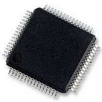
UPD78F0890GK(A)-GAJ-AX NEC, UPD78F0890GK(A)-GAJ-AX Datasheet - Page 520

UPD78F0890GK(A)-GAJ-AX
Manufacturer Part Number
UPD78F0890GK(A)-GAJ-AX
Description
8BIT MCU, 128K FLASH, 7K RAM, LQFP
Manufacturer
NEC
Datasheet
1.UPD78F0890GKA-GAJ-AX.pdf
(732 pages)
Specifications of UPD78F0890GK(A)-GAJ-AX
Controller Family/series
UPD78F
No. Of I/o's
55
Ram Memory Size
7KB
Cpu Speed
20MHz
No. Of Timers
10
No. Of Pwm
RoHS Compliant
Core Size
8bit
Program Memory Size
128KB
Oscillator Type
External, Internal
- Current page: 520 of 732
- Download datasheet (4Mb)
<R>
520
Maskable
Software
Reset
Notes 1. The default priority is the priority applicable when two or more maskable interrupt are generated
Interrupt
Type
2. Basic configuration types (A) to (C) correspond to (A) to (C) in Figure 17-1.
3. When the 8-bit timer/event counter 51 is used in the carrier generator mode, the interrupt source is
4. When bit 1 (LVIMD) of the low-voltage detection register (LVIM) is set to 1.
simultaneously. 0 is the highest priority, and 28 is the lowest.
INTTM5H1 (see Figure 9-13 Transfer Timing).
Priority
Default
17
18
19
20
21
22
23
24
25
26
27
28
−
−
Note 1
INTTMH1
INTTMH0
INTTM50
INTTM000
INTTM010
INTAD
INTWTI
INTDMU
INTTM51
INTWT
INTCSI11
INTTM001
INTTM011
BRK
RESET
POC
LVI
WDT
Name
Note 3
Table 17-1. Interrupt Source List (2/2)
CHAPTER 17 INTERRUPT FUNCTIONS
Match between TMH1 and CMP01
(when compare register is specified)
Match between TMH0 and CMP00
(when compare register is specified)
Match between TM50 and CR50
(when compare register is specified)
Match between TM00 and CR000
(when compare register is specified),
TI010 pin valid edge detection
(when capture register is specified)
Match between TM00 and CR010
(when compare register is specified),
TI000 pin valid edge detection
(when capture register is specified)
End of A/D conversion
Watch timer reference time interval signal
DMU operation end
Match between TM51 and CR51
(when compare register is specified)
Watch timer overflow
End of CSI11 communication
Match between TM01 and CR001 (when
compare register is specified), TI011 pin
valid edge detection (when capture register
is specified)
Match between TM01 and CR011 (when
compare register is specified), TI001 pin
valid edge detection (when capture register
is specified)
BRK instruction execution
Reset input
Power-on clear
Low-voltage detection
WDT overflow
Interrupt Source
User’s Manual U17554EJ4V0UD
Trigger
Note 4
Internal
Internal/
External
−
−
Address
002CH
003CH
002AH
002EH
003AH
003EH
Vector
0026H
0028H
0030H
0032H
0034H
0036H
0038H
0000H
Table
Configuration
Type
Basic
(A)
(C)
−
Note 2
Related parts for UPD78F0890GK(A)-GAJ-AX
Image
Part Number
Description
Manufacturer
Datasheet
Request
R

Part Number:
Description:
16/8 bit single-chip microcomputer
Manufacturer:
NEC
Datasheet:

Part Number:
Description:
Dual audio power amp circuit
Manufacturer:
NEC
Datasheet:

Part Number:
Description:
Dual comparator
Manufacturer:
NEC
Datasheet:

Part Number:
Description:
MOS type composite field effect transistor
Manufacturer:
NEC
Datasheet:

Part Number:
Description:
50 V/100 mA FET array incorporating 2 N-ch MOSFETs
Manufacturer:
NEC
Datasheet:

Part Number:
Description:
6-pin small MM high-frequency double transistor
Manufacturer:
NEC
Datasheet:

Part Number:
Description:
6-pin small MM high-frequency double transistor
Manufacturer:
NEC
Datasheet:

Part Number:
Description:
6-pin small MM high-frequency double transistor
Manufacturer:
NEC
Datasheet:

Part Number:
Description:
6-pin small MM high-frequency double transistor
Manufacturer:
NEC
Datasheet:

Part Number:
Description:
Twin transistors equipped with different model chips(6P small MM)
Manufacturer:
NEC
Datasheet:

Part Number:
Description:
Bipolar analog integrated circuit
Manufacturer:
NEC
Datasheet:


