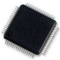
UPD78F0890GK(A)-GAJ-AX NEC, UPD78F0890GK(A)-GAJ-AX Datasheet - Page 359

UPD78F0890GK(A)-GAJ-AX
Manufacturer Part Number
UPD78F0890GK(A)-GAJ-AX
Description
8BIT MCU, 128K FLASH, 7K RAM, LQFP
Manufacturer
NEC
Datasheet
1.UPD78F0890GKA-GAJ-AX.pdf
(732 pages)
Specifications of UPD78F0890GK(A)-GAJ-AX
Controller Family/series
UPD78F
No. Of I/o's
55
Ram Memory Size
7KB
Cpu Speed
20MHz
No. Of Timers
10
No. Of Pwm
RoHS Compliant
Core Size
8bit
Program Memory Size
128KB
Oscillator Type
External, Internal
- Current page: 359 of 732
- Download datasheet (4Mb)
(1) Transmit buffer register 1n (SOTB1n)
(2) Serial I/O shift register 1n (SIO1n)
SCK11/P76
Remark (a): SO11 output
This register sets the transmit data.
Transmission/reception is started by writing data to SOTB1n when bit 7 (CSIE1n) and bit 6 (TRMD1n) of serial
operation mode register 1n (CSIM1n) is 1.
The data written to SOTB1n is converted from parallel data into serial data by serial I/O shift register 1n, and
output to the serial output pin (SO1n).
SOTB1n can be written or read by an 8-bit memory manipulation instruction.
Reset signal generation clears this register to 00H.
This is an 8-bit register that converts data from parallel data into serial data and vice versa.
This register can be read by an 8-bit memory manipulation instruction.
Reception is started by reading data from SIO1n if bit 6 (TRMD1n) of serial operation mode register 1n (CSIM1n)
is 0.
During reception, the data is read from the serial input pin (SI1n) to SIO1n.
Reset signal generation clears this register to 00H.
Cautions 1. Do not access SOTB1n when CSOT1n = 1 (during serial communication).
Cautions 1. Do not access SIO1n when CSOT1n = 1 (during serial communication).
Remark
SI11/P75
f
f
f
f
f
f
SSI11
PRS
PRS
PRS
PRS
PRS
PRS
f
PRS
/2
/2
/2
/2
/2
/2
2. In the slave mode, transmission/reception is started when data is written to SOTB11 with
2. In the slave mode, reception is started when data is read from SIO11 with a low level input
n = 0, 1
/2
2
3
4
5
6
7
a low level input to the SSI11 pin. For details of the transmission/reception operation, see
15.4.2 (2) Communication operation.
to the SSI11 pin. For details of the reception operation, see 15.4.2 (2) Communication
operation.
PM04
Transmit data
controller
Figure 15-2. Block Diagram of Serial Interface CSI11
CHAPTER 15 SERIAL INTERFACES CSI10 AND CSI11
Serial I/O shift
register 11 (SIO11)
Output latch
Clock start/stop controller &
(P04)
clock phase controller
Transmit controller
8
Baud rate generator
Internal bus
User’s Manual U17554EJ4V0UD
Output latch
Transmit buffer
register 11 (SOTB11)
8
selector
Output
INTCSI11
(a)
Output latch
(P74)
PM74
SSI11
SO11/P74
359
Related parts for UPD78F0890GK(A)-GAJ-AX
Image
Part Number
Description
Manufacturer
Datasheet
Request
R

Part Number:
Description:
16/8 bit single-chip microcomputer
Manufacturer:
NEC
Datasheet:

Part Number:
Description:
Dual audio power amp circuit
Manufacturer:
NEC
Datasheet:

Part Number:
Description:
Dual comparator
Manufacturer:
NEC
Datasheet:

Part Number:
Description:
MOS type composite field effect transistor
Manufacturer:
NEC
Datasheet:

Part Number:
Description:
50 V/100 mA FET array incorporating 2 N-ch MOSFETs
Manufacturer:
NEC
Datasheet:

Part Number:
Description:
6-pin small MM high-frequency double transistor
Manufacturer:
NEC
Datasheet:

Part Number:
Description:
6-pin small MM high-frequency double transistor
Manufacturer:
NEC
Datasheet:

Part Number:
Description:
6-pin small MM high-frequency double transistor
Manufacturer:
NEC
Datasheet:

Part Number:
Description:
6-pin small MM high-frequency double transistor
Manufacturer:
NEC
Datasheet:

Part Number:
Description:
Twin transistors equipped with different model chips(6P small MM)
Manufacturer:
NEC
Datasheet:

Part Number:
Description:
Bipolar analog integrated circuit
Manufacturer:
NEC
Datasheet:


