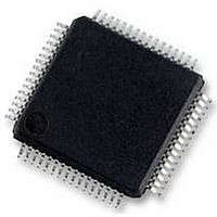
UPD78F0890GK(A)-GAJ-AX NEC, UPD78F0890GK(A)-GAJ-AX Datasheet - Page 607

UPD78F0890GK(A)-GAJ-AX
Manufacturer Part Number
UPD78F0890GK(A)-GAJ-AX
Description
8BIT MCU, 128K FLASH, 7K RAM, LQFP
Manufacturer
NEC
Datasheet
1.UPD78F0890GKA-GAJ-AX.pdf
(732 pages)
Specifications of UPD78F0890GK(A)-GAJ-AX
Controller Family/series
UPD78F
No. Of I/o's
55
Ram Memory Size
7KB
Cpu Speed
20MHz
No. Of Timers
10
No. Of Pwm
RoHS Compliant
Core Size
8bit
Program Memory Size
128KB
Oscillator Type
External, Internal
- Current page: 607 of 732
- Download datasheet (4Mb)
24.6 Connection of Pins on Board
provided on the target system. First provide a function that selects the normal operation mode or flash memory
programming mode on the board.
the same status as immediately after reset. Therefore, if the external device does not recognize the state immediately
after reset, the pins must be handled as described below.
24.6.1 FLMD0 pin
write voltage is supplied to the FLMD0 pin. An FLMD0 pin connection example is shown below.
24.6.2 Serial interface pins
device on the board, care must be exercised so that signals do not collide or that the other device does not
malfunction.
To write the flash memory on-board, connectors that connect the dedicated flash memory programmer must be
When the flash memory programming mode is set, all the pins not used for programming the flash memory are in
In the normal operation mode, 0 V is input to the FLMD0 pin. In the flash memory programming mode, the V
The pins used by each serial interface are listed below.
To connect the dedicated flash memory programmer to the pins of a serial interface that is connected to another
CSI10
UART60
78K0/FE2
FLMD0
Table 24-5. Pins Used by Each Serial Interface
Figure 24-8. FLMD0 Pin Connection Example
Serial Interface
CHAPTER 24 FLASH MEMORY
User’s Manual U17554EJ4V0UD
10 k (recommended)
Dedicated flash memory programmer
connection pin
SO10, SI10, SCK10
TxD60, RxD60
Pins Used
607
DD
Related parts for UPD78F0890GK(A)-GAJ-AX
Image
Part Number
Description
Manufacturer
Datasheet
Request
R

Part Number:
Description:
16/8 bit single-chip microcomputer
Manufacturer:
NEC
Datasheet:

Part Number:
Description:
Dual audio power amp circuit
Manufacturer:
NEC
Datasheet:

Part Number:
Description:
Dual comparator
Manufacturer:
NEC
Datasheet:

Part Number:
Description:
MOS type composite field effect transistor
Manufacturer:
NEC
Datasheet:

Part Number:
Description:
50 V/100 mA FET array incorporating 2 N-ch MOSFETs
Manufacturer:
NEC
Datasheet:

Part Number:
Description:
6-pin small MM high-frequency double transistor
Manufacturer:
NEC
Datasheet:

Part Number:
Description:
6-pin small MM high-frequency double transistor
Manufacturer:
NEC
Datasheet:

Part Number:
Description:
6-pin small MM high-frequency double transistor
Manufacturer:
NEC
Datasheet:

Part Number:
Description:
6-pin small MM high-frequency double transistor
Manufacturer:
NEC
Datasheet:

Part Number:
Description:
Twin transistors equipped with different model chips(6P small MM)
Manufacturer:
NEC
Datasheet:

Part Number:
Description:
Bipolar analog integrated circuit
Manufacturer:
NEC
Datasheet:


