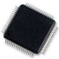
UPD78F0890GK(A)-GAJ-AX NEC, UPD78F0890GK(A)-GAJ-AX Datasheet - Page 261

UPD78F0890GK(A)-GAJ-AX
Manufacturer Part Number
UPD78F0890GK(A)-GAJ-AX
Description
8BIT MCU, 128K FLASH, 7K RAM, LQFP
Manufacturer
NEC
Datasheet
1.UPD78F0890GKA-GAJ-AX.pdf
(732 pages)
Specifications of UPD78F0890GK(A)-GAJ-AX
Controller Family/series
UPD78F
No. Of I/o's
55
Ram Memory Size
7KB
Cpu Speed
20MHz
No. Of Timers
10
No. Of Pwm
RoHS Compliant
Core Size
8bit
Program Memory Size
128KB
Oscillator Type
External, Internal
- Current page: 261 of 732
- Download datasheet (4Mb)
(4) Timing chart
If the setting value of the CMP01 register is N, the setting value of the CMP11 register is M, and the count clock
frequency is f
The carrier output control timing is shown below.
Cautions 1. Be sure to set the CMP11 register when starting the timer count operation (TMHE1 = 1)
Cautions 1. Set the values of the CMP01 and CMP11 registers in a range of 01H to FFH.
2. Set so that the count clock frequency of TMH1 becomes more than 6 times the count clock
2. In the carrier generator mode, three operating clocks (signal selected by CKS12 to CKS10
3. Be sure to set the RMC1 bit before the count operation is started.
CNT
after the timer count operation was stopped (TMHE1 = 0) (be sure to set again even if
setting the same value to the CMP11 register).
frequency of TM51.
bits of TMHMD1 register) or more are required from when the CMP11 register value is
changed to when the value is transferred to the register.
, the carrier clock output cycle and duty are as follows.
Carrier clock output cycle = (N + M + 2)/f
Duty = High-level width : Carrier clock output width = ( M + 1) : (N + M + 2)
CHAPTER 9 8-BIT TIMERS H0 AND H1
User’s Manual U17554EJ4V0UD
CNT
261
Related parts for UPD78F0890GK(A)-GAJ-AX
Image
Part Number
Description
Manufacturer
Datasheet
Request
R

Part Number:
Description:
16/8 bit single-chip microcomputer
Manufacturer:
NEC
Datasheet:

Part Number:
Description:
Dual audio power amp circuit
Manufacturer:
NEC
Datasheet:

Part Number:
Description:
Dual comparator
Manufacturer:
NEC
Datasheet:

Part Number:
Description:
MOS type composite field effect transistor
Manufacturer:
NEC
Datasheet:

Part Number:
Description:
50 V/100 mA FET array incorporating 2 N-ch MOSFETs
Manufacturer:
NEC
Datasheet:

Part Number:
Description:
6-pin small MM high-frequency double transistor
Manufacturer:
NEC
Datasheet:

Part Number:
Description:
6-pin small MM high-frequency double transistor
Manufacturer:
NEC
Datasheet:

Part Number:
Description:
6-pin small MM high-frequency double transistor
Manufacturer:
NEC
Datasheet:

Part Number:
Description:
6-pin small MM high-frequency double transistor
Manufacturer:
NEC
Datasheet:

Part Number:
Description:
Twin transistors equipped with different model chips(6P small MM)
Manufacturer:
NEC
Datasheet:

Part Number:
Description:
Bipolar analog integrated circuit
Manufacturer:
NEC
Datasheet:


