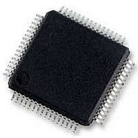
UPD78F0890GK(A)-GAJ-AX NEC, UPD78F0890GK(A)-GAJ-AX Datasheet - Page 354

UPD78F0890GK(A)-GAJ-AX
Manufacturer Part Number
UPD78F0890GK(A)-GAJ-AX
Description
8BIT MCU, 128K FLASH, 7K RAM, LQFP
Manufacturer
NEC
Datasheet
1.UPD78F0890GKA-GAJ-AX.pdf
(732 pages)
Specifications of UPD78F0890GK(A)-GAJ-AX
Controller Family/series
UPD78F
No. Of I/o's
55
Ram Memory Size
7KB
Cpu Speed
20MHz
No. Of Timers
10
No. Of Pwm
RoHS Compliant
Core Size
8bit
Program Memory Size
128KB
Oscillator Type
External, Internal
- Current page: 354 of 732
- Download datasheet (4Mb)
(4) Permissible baud rate range during reception
354
The permissible error from the baud rate at the transmission destination during reception is shown below.
As shown in Figure 14-33, the latch timing of the receive data is determined by the counter set by baud rate
generator control register 6n (BRGC6n) after the start bit has been detected. If the last data (stop bit) meets this
latch timing, the data can be correctly received.
Assuming that 11-bit data is received, the theoretical values can be calculated as follows.
Caution Make sure that the baud rate error during reception is within the permissible error range, by
Remark n = 0, 1
UART60 and UART61
Maximum permissible
FL = (Brate)
Minimum permissible
Data frame lengtz of
Brate: Baud rate of UART60 and UART61
k:
FL:
Margin of latch timing: 2 clocks
data frame length
data frame length
using the calculation expression shown below.
Set value of BRGC6n
1-bit data length
−
1
Figure 14-33. Permissible Baud Rate Range During Reception
CHAPTER 14 SERIAL INTERFACES UART60 AND UART61
Latch timing
Start bit
Start bit
Start bit
User’s Manual U17554EJ4V0UD
Bit 0
Bit 0
FL
Bit 0
Bit 1
Bit 1
Bit 1
1 data frame (11
FLmin
FLmax
Bit 7
Bit 7
FL)
Bit 7
Parity bit
Parity bit
Parity bit
Stop bit
Stop bit
Stop bit
Related parts for UPD78F0890GK(A)-GAJ-AX
Image
Part Number
Description
Manufacturer
Datasheet
Request
R

Part Number:
Description:
16/8 bit single-chip microcomputer
Manufacturer:
NEC
Datasheet:

Part Number:
Description:
Dual audio power amp circuit
Manufacturer:
NEC
Datasheet:

Part Number:
Description:
Dual comparator
Manufacturer:
NEC
Datasheet:

Part Number:
Description:
MOS type composite field effect transistor
Manufacturer:
NEC
Datasheet:

Part Number:
Description:
50 V/100 mA FET array incorporating 2 N-ch MOSFETs
Manufacturer:
NEC
Datasheet:

Part Number:
Description:
6-pin small MM high-frequency double transistor
Manufacturer:
NEC
Datasheet:

Part Number:
Description:
6-pin small MM high-frequency double transistor
Manufacturer:
NEC
Datasheet:

Part Number:
Description:
6-pin small MM high-frequency double transistor
Manufacturer:
NEC
Datasheet:

Part Number:
Description:
6-pin small MM high-frequency double transistor
Manufacturer:
NEC
Datasheet:

Part Number:
Description:
Twin transistors equipped with different model chips(6P small MM)
Manufacturer:
NEC
Datasheet:

Part Number:
Description:
Bipolar analog integrated circuit
Manufacturer:
NEC
Datasheet:


