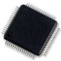
UPD78F0890GK(A)-GAJ-AX NEC, UPD78F0890GK(A)-GAJ-AX Datasheet - Page 698

UPD78F0890GK(A)-GAJ-AX
Manufacturer Part Number
UPD78F0890GK(A)-GAJ-AX
Description
8BIT MCU, 128K FLASH, 7K RAM, LQFP
Manufacturer
NEC
Datasheet
1.UPD78F0890GKA-GAJ-AX.pdf
(732 pages)
Specifications of UPD78F0890GK(A)-GAJ-AX
Controller Family/series
UPD78F
No. Of I/o's
55
Ram Memory Size
7KB
Cpu Speed
20MHz
No. Of Timers
10
No. Of Pwm
RoHS Compliant
Core Size
8bit
Program Memory Size
128KB
Oscillator Type
External, Internal
- Current page: 698 of 732
- Download datasheet (4Mb)
Caution When Value is Φ
Remark F
698
CAN
Peripheral
Hardware
F
F
VPCLK
VPSTB
CANCLK
Global Reg.
CANmodule
Reg.
C0RGPT
C0LIPT
C0TGPT
C0LOPT
Message Buf.
Message Buf.
Message Buf.
:
:
: AFCAN macro frequency
Table 31-2 RAM Access That Generate Wait and Number of CPU Wait Clocks
Register
VPCLK frequency
VPSTB frequency
CANMOD
Read/Write
Read
Write(8 bit)
Write(16 bit)
(CAN module system clock) ≥ 2 MHz.
Access
CHAPTER 31 CAUTIONS FOR WAIT
User’s Manual U17554EJ4V0UD
number of wait clocks
MIN.
1
2
2
1
MAX.
14
17
11
1
synchronizaition of NPB signals with VPCLK
<Calculating number of wait clocks>
MIN. ROUNDUP[(1/F
MAX. ROUNDUP[(1/F
Synchronization of NPB signals with VPCLK
RAM access delay (1 RAM - RD access)
<Calculating number of wait clocks>
MIN. ROUNDUP[(1/F
MAX. ROUNDUP[(1/F
synchronization of NPB signals with VPCLK
RAM access delay (1RAM - RD + 1RAM - WR
access)
<Calculating number of wait clocks>
MIN. ROUNDUP[(1/F
MAX. ROUNDUP[(1/F
synchronization of NPB signals with VPCLK
RAM access delay (1 RAM - WR access)
<Calculating number of wait clocks>
MIN. ROUNDUP[(1/F
MAX. ROUNDUP[(1/F
Cause
VPCLK
CANCLK
CANCLK
CANCLK
VPCLK
CANCLK
CANCLK
CANCLK
) × 1/(1/F
) × 2/(1/F
) × 3/(1/F
) × 4/(1/F
) × 2/(1/F
) × 4/(1/F
) × 5/(1/F
) × 3/(1/F
VPSTB
VPSTB
VPSTB
VPSTB
VPSTB
VPSTB
VPSTB
VPSTB
)]
)]
)]
)]
)]
)]
)]
)]
Related parts for UPD78F0890GK(A)-GAJ-AX
Image
Part Number
Description
Manufacturer
Datasheet
Request
R

Part Number:
Description:
16/8 bit single-chip microcomputer
Manufacturer:
NEC
Datasheet:

Part Number:
Description:
Dual audio power amp circuit
Manufacturer:
NEC
Datasheet:

Part Number:
Description:
Dual comparator
Manufacturer:
NEC
Datasheet:

Part Number:
Description:
MOS type composite field effect transistor
Manufacturer:
NEC
Datasheet:

Part Number:
Description:
50 V/100 mA FET array incorporating 2 N-ch MOSFETs
Manufacturer:
NEC
Datasheet:

Part Number:
Description:
6-pin small MM high-frequency double transistor
Manufacturer:
NEC
Datasheet:

Part Number:
Description:
6-pin small MM high-frequency double transistor
Manufacturer:
NEC
Datasheet:

Part Number:
Description:
6-pin small MM high-frequency double transistor
Manufacturer:
NEC
Datasheet:

Part Number:
Description:
6-pin small MM high-frequency double transistor
Manufacturer:
NEC
Datasheet:

Part Number:
Description:
Twin transistors equipped with different model chips(6P small MM)
Manufacturer:
NEC
Datasheet:

Part Number:
Description:
Bipolar analog integrated circuit
Manufacturer:
NEC
Datasheet:


