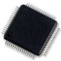
UPD78F0890GK(A)-GAJ-AX NEC, UPD78F0890GK(A)-GAJ-AX Datasheet - Page 304

UPD78F0890GK(A)-GAJ-AX
Manufacturer Part Number
UPD78F0890GK(A)-GAJ-AX
Description
8BIT MCU, 128K FLASH, 7K RAM, LQFP
Manufacturer
NEC
Datasheet
1.UPD78F0890GKA-GAJ-AX.pdf
(732 pages)
Specifications of UPD78F0890GK(A)-GAJ-AX
Controller Family/series
UPD78F
No. Of I/o's
55
Ram Memory Size
7KB
Cpu Speed
20MHz
No. Of Timers
10
No. Of Pwm
RoHS Compliant
Core Size
8bit
Program Memory Size
128KB
Oscillator Type
External, Internal
- Current page: 304 of 732
- Download datasheet (4Mb)
(5) P80/ANI0 to P87/ANI7, P90/ANI8 to P93/ANI11
(6) Input impedance of ANI0 to ANI11 pins
(7) AV
304
<1> The analog input pins (ANI0 to ANI11) are also used as I/O port pins (P80 to P87, P90 to P93).
<2> If a digital pulse is applied to the pins adjacent to the pins currently used for A/D conversion, the expected
This A/D converter charges a sampling capacitor for sampling during sampling time.
Therefore, only a leakage current flows when sampling is not in progress, and a current that charges the
capacitor flows during sampling. Consequently, the input impedance fluctuates depending on whether sampling
is in progress, and on the other states.
To make sure that sampling is effective, however, it is recommended to keep the output impedance of the analog
input source to within 10 kΩ, and to connect a capacitor of about 100 pF to the ANI0 to ANI11 pins (see Figure
13-21).
A series resistor string of several tens of kΩ is connected between the AV
Therefore, if the output impedance of the reference voltage source is high, this will result in a series connection to
the series resistor string between the AV
Reference
C = 100 to 1,000 pF
voltage
REF
input
When A/D conversion is performed with any of ANI0 to ANI11 selected, do not access P80 to P87, P90 to
P93 while conversion is in progress; otherwise the conversion resolution may be degraded.
recommended to select pins used as P80 to P87, P90 to P93 starting with the P80/ANI0 that is the furthest
from AV
value of the A/D conversion may not be obtained due to coupling noise. Therefore, do not apply a pulse to
the pins adjacent to the pin undergoing A/D conversion.
pin input impedance
REF
.
Figure 13-21. Analog Input Pin Connection
CHAPTER 13 A/D CONVERTER
REF
User’s Manual U17554EJ4V0UD
and AV
AV
AV
V
ANI0 to ANI11
SS
REF
SS
If there is a possibility that noise equal to or higher than AV
equal to or lower than AV
small V
SS
pins, resulting in a large reference voltage error.
F
value (0.3 V or lower).
SS
REF
may enter, clamp with a diode with a
and AV
SS
pins.
REF
or
It is
Related parts for UPD78F0890GK(A)-GAJ-AX
Image
Part Number
Description
Manufacturer
Datasheet
Request
R

Part Number:
Description:
16/8 bit single-chip microcomputer
Manufacturer:
NEC
Datasheet:

Part Number:
Description:
Dual audio power amp circuit
Manufacturer:
NEC
Datasheet:

Part Number:
Description:
Dual comparator
Manufacturer:
NEC
Datasheet:

Part Number:
Description:
MOS type composite field effect transistor
Manufacturer:
NEC
Datasheet:

Part Number:
Description:
50 V/100 mA FET array incorporating 2 N-ch MOSFETs
Manufacturer:
NEC
Datasheet:

Part Number:
Description:
6-pin small MM high-frequency double transistor
Manufacturer:
NEC
Datasheet:

Part Number:
Description:
6-pin small MM high-frequency double transistor
Manufacturer:
NEC
Datasheet:

Part Number:
Description:
6-pin small MM high-frequency double transistor
Manufacturer:
NEC
Datasheet:

Part Number:
Description:
6-pin small MM high-frequency double transistor
Manufacturer:
NEC
Datasheet:

Part Number:
Description:
Twin transistors equipped with different model chips(6P small MM)
Manufacturer:
NEC
Datasheet:

Part Number:
Description:
Bipolar analog integrated circuit
Manufacturer:
NEC
Datasheet:


