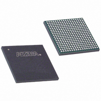
EP3C25F324I7 Altera, EP3C25F324I7 Datasheet - Page 105

EP3C25F324I7
Manufacturer Part Number
EP3C25F324I7
Description
IC CYCLONE III FPGA 25K 324 FBGA
Manufacturer
Altera
Series
Cyclone® IIIr
Datasheets
1.EP3C5F256C8N.pdf
(5 pages)
2.EP3C5F256C8N.pdf
(34 pages)
3.EP3C5F256C8N.pdf
(66 pages)
4.EP3C5F256C8N.pdf
(14 pages)
5.EP3C5F256C8N.pdf
(76 pages)
6.EP3C25F324I7.pdf
(274 pages)
Specifications of EP3C25F324I7
Number Of Logic Elements/cells
24624
Number Of Labs/clbs
1539
Total Ram Bits
608256
Number Of I /o
215
Voltage - Supply
1.15 V ~ 1.25 V
Mounting Type
Surface Mount
Operating Temperature
-40°C ~ 100°C
Package / Case
324-FBGA
Family Name
Cyclone III
Number Of Logic Blocks/elements
24624
# I/os (max)
215
Frequency (max)
437.5MHz
Process Technology
65nm
Operating Supply Voltage (typ)
1.2V
Logic Cells
24624
Ram Bits
608256
Operating Supply Voltage (min)
1.15V
Operating Supply Voltage (max)
1.25V
Operating Temp Range
-40C to 100C
Operating Temperature Classification
Industrial
Mounting
Surface Mount
Pin Count
324
Package Type
FBGA
For Use With
544-2370 - KIT STARTER CYCLONE III EP3C25
Lead Free Status / RoHS Status
Contains lead / RoHS non-compliant
Number Of Gates
-
Lead Free Status / Rohs Status
Not Compliant
Available stocks
Company
Part Number
Manufacturer
Quantity
Price
Company:
Part Number:
EP3C25F324I7N
Manufacturer:
ALTERA32
Quantity:
181
Chapter 6: I/O Features in the Cyclone III Device Family
I/O Element Features
Programmable Pull-Up Resistor
Programmable Delay
© December 2009
f
f
f
1
Altera Corporation
For more information, refer to the
Quartus II Handbook.
For the specific sustaining current for each V
resistor and for the overdrive current used to identify the next driven input level,
refer to the
Each Cyclone III device family I/O pin provides an optional programmable pull-up
resistor while in user mode. If you enable this feature for an I/O pin, the pull-up
resistor holds the output to the V
If you enable the programmable pull-up, the device cannot use the bus-hold feature.
Programmable pull-up resistors are not supported on the dedicated configuration,
JTAG, and dedicated clock pins.
For more information, refer to the
Quartus II Handbook.
The Cyclone III device family IOE includes programmable delays to ensure zero hold
times, minimize setup times, increase clock-to-output times, or delay the clock input
signal.
A path in which a pin directly drives a register may require a programmable delay to
ensure zero hold time, whereas a path in which a pin drives a register through
combinational logic may not require the delay. Programmable delays minimize setup
time. The Quartus II Compiler can program these delays to automatically minimize
setup time while providing a zero hold time. Programmable delays can increase the
register-to-pin delays for output registers. Each dual-purpose clock input pin
provides a programmable delay to the global clock networks.
Table 6–2
Table 6–2. Cyclone III Device Family Programmable Delay Chain
There are two paths in the IOE for an input to reach the logic array. Each of the two
paths can have a different delay. This allows you to adjust delays from the pin to the
internal logic element (LE) registers that reside in two different areas of the device.
You must set the two combinational input delays with the input delay from pin to
internal cells logic option in the Quartus II software for each path. If the pin uses the
input register, one of the delays is disregarded and the delay is set with the input
delay from pin to input register logic option in the Quartus II software.
Input pin-to-logic array delay
Input pin-to-input register delay
Output pin delay
Dual-purpose clock input pin
delay
Programmable Delays
lists the programmable delays for the Cyclone III device family.
Cyclone III Device Data Sheet
Input delay from pin to internal cells
Input delay from pin to input register
Delay from output register to output pin
Input delay from dual-purpose clock pin to fan-out destinations
CCIO
Assignment Editor
Assignment Editor
level of the output pin’s bank.
and
Cyclone III LS Device Data Sheet
CCIO
Quartus II Logic Option
voltage level driven through the
chapter in volume 2 of the
chapter in volume 2 of the
Cyclone III Device Handbook, Volume 1
chapters.
6–5


