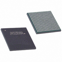
EP3C25F324I7 Altera, EP3C25F324I7 Datasheet - Page 199

EP3C25F324I7
Manufacturer Part Number
EP3C25F324I7
Description
IC CYCLONE III FPGA 25K 324 FBGA
Manufacturer
Altera
Series
Cyclone® IIIr
Datasheets
1.EP3C5F256C8N.pdf
(5 pages)
2.EP3C5F256C8N.pdf
(34 pages)
3.EP3C5F256C8N.pdf
(66 pages)
4.EP3C5F256C8N.pdf
(14 pages)
5.EP3C5F256C8N.pdf
(76 pages)
6.EP3C25F324I7.pdf
(274 pages)
Specifications of EP3C25F324I7
Number Of Logic Elements/cells
24624
Number Of Labs/clbs
1539
Total Ram Bits
608256
Number Of I /o
215
Voltage - Supply
1.15 V ~ 1.25 V
Mounting Type
Surface Mount
Operating Temperature
-40°C ~ 100°C
Package / Case
324-FBGA
Family Name
Cyclone III
Number Of Logic Blocks/elements
24624
# I/os (max)
215
Frequency (max)
437.5MHz
Process Technology
65nm
Operating Supply Voltage (typ)
1.2V
Logic Cells
24624
Ram Bits
608256
Operating Supply Voltage (min)
1.15V
Operating Supply Voltage (max)
1.25V
Operating Temp Range
-40C to 100C
Operating Temperature Classification
Industrial
Mounting
Surface Mount
Pin Count
324
Package Type
FBGA
For Use With
544-2370 - KIT STARTER CYCLONE III EP3C25
Lead Free Status / RoHS Status
Contains lead / RoHS non-compliant
Number Of Gates
-
Lead Free Status / Rohs Status
Not Compliant
Available stocks
Company
Part Number
Manufacturer
Quantity
Price
Company:
Part Number:
EP3C25F324I7N
Manufacturer:
ALTERA32
Quantity:
181
Chapter 9: Configuration, Design Security, and Remote System Upgrades in the Cyclone III Device Family
Configuration Features
Table 9–13. PS Configuration Timing Parameters for Cyclone III Device Family
© December 2009
t
t
t
t
t
t
t
t
t
t
t
t
Symbol
CF 2CD
CF 2ST0
CF G
STATUS
CF 2ST1
CF 2CK
ST2C K
DSU
DH
CH
CL
CLK
nCONFIG low to CONF_DONE low
nCONFIG low to nSTATUS low
nCONFIG low pulse width
nSTATUS low pulse width
nCONFIG high to nSTATUS high
nCONFIG high to first rising edge on DCLK
nSTATUS high to first rising edge of DCLK
Data setup time before rising edge on
Data hold time after rising edge on
DCLK high time
DCLK low time
DCLK period
Altera Corporation
PS Configuration Timing
A PS configuration must meet the setup and hold timing parameters and the
maximum clock frequency. When using a microprocessor or another intelligent host
to control the PS interface, ensure that you meet these timing requirements.
Figure 9–17
external host device as an external host.
Figure 9–17. PS Configuration Timing Waveform
Notes to
(1) The beginning of this waveform shows the device in user mode. In user mode, nCONFIG, nSTATUS, and
(2) After power-up, the Cyclone III device family holds nSTATUS low during POR delay.
(3) After power-up, before and during configuration, CONF_DONE is low.
(4) In user mode, drive DCLK either high or low when using the PS configuration scheme, whichever is more convenient.
(5) Do not leave the DATA[0] pin floating after configuration. Drive it high or low, whichever is more convenient.
Table 9–13
CONF_DONE are at logic-high levels. When nCONFIG is pulled low, a reconfiguration cycle begins.
When using the AS configuration scheme, DCLK is a Cyclone III device family output pin and must not be driven
externally.
Figure
Parameter
CONF_DONE (3)
lists the PS configuration timing parameters for Cyclone III device family.
nSTATUS (2)
shows the timing waveform for a PS configuration when using an
INIT_DONE
9–17:
nCONFIG
DCLK (4)
User I/O
DATA[0]
DCLK
Tri-stated with internal pull-up resistor
DCLK
t
t
CFG
CF2CD
t
CF2ST1
t
CF2ST0
t
CF2CK
t
ST2CK
t
Bit 0 Bit 1 Bit 2 Bit 3
STATUS
t
CH
t
CLK
t
DSU
t
CL
t
DH
(Note 1)
(Note 1)
Minimum
230
500
3.2
3.2
7.5
—
—
45
—
2
5
0
Bit n
(2)
(Part 1 of 2)
Cyclone III Device Handbook, Volume 1
t
CD2UM
Maximum
230
230
User Mode
500
500
(5)
—
—
—
—
—
—
—
—
(2)
(2)
Unit
ns
ns
ns
μs
μs
μs
μs
ns
ns
ns
ns
ns
9–39


