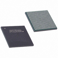
EP3C25F324I7 Altera, EP3C25F324I7 Datasheet - Page 179

EP3C25F324I7
Manufacturer Part Number
EP3C25F324I7
Description
IC CYCLONE III FPGA 25K 324 FBGA
Manufacturer
Altera
Series
Cyclone® IIIr
Datasheets
1.EP3C5F256C8N.pdf
(5 pages)
2.EP3C5F256C8N.pdf
(34 pages)
3.EP3C5F256C8N.pdf
(66 pages)
4.EP3C5F256C8N.pdf
(14 pages)
5.EP3C5F256C8N.pdf
(76 pages)
6.EP3C25F324I7.pdf
(274 pages)
Specifications of EP3C25F324I7
Number Of Logic Elements/cells
24624
Number Of Labs/clbs
1539
Total Ram Bits
608256
Number Of I /o
215
Voltage - Supply
1.15 V ~ 1.25 V
Mounting Type
Surface Mount
Operating Temperature
-40°C ~ 100°C
Package / Case
324-FBGA
Family Name
Cyclone III
Number Of Logic Blocks/elements
24624
# I/os (max)
215
Frequency (max)
437.5MHz
Process Technology
65nm
Operating Supply Voltage (typ)
1.2V
Logic Cells
24624
Ram Bits
608256
Operating Supply Voltage (min)
1.15V
Operating Supply Voltage (max)
1.25V
Operating Temp Range
-40C to 100C
Operating Temperature Classification
Industrial
Mounting
Surface Mount
Pin Count
324
Package Type
FBGA
For Use With
544-2370 - KIT STARTER CYCLONE III EP3C25
Lead Free Status / RoHS Status
Contains lead / RoHS non-compliant
Number Of Gates
-
Lead Free Status / Rohs Status
Not Compliant
Available stocks
Company
Part Number
Manufacturer
Quantity
Price
Company:
Part Number:
EP3C25F324I7N
Manufacturer:
ALTERA32
Quantity:
181
Chapter 9: Configuration, Design Security, and Remote System Upgrades in the Cyclone III Device Family
Configuration Features
Figure 9–6. Multi-Device AS Configuration where the Devices Receive the Same Data with a Single .sof
Notes to
(1) Connect the pull-up resistors to the V
(2) The nCEO pin is left unconnected or used as a user I/O pin when it does not feed the nCE pin of another device.
(3) The MSEL pin settings vary for different configuration voltage standards and POR time. You must set the master device of the Cyclone III device
(4) These are dual-purpose I/O pins. The nCSO pin functions as the FLASH_NCE pin in AP mode. The ASDO pin functions as the DATA[1] pin in
(5) Connect the series resistor at the near end of the serial configuration device.
(6) Connect the repeater buffers between the master and slave devices for DATA[0] and DCLK. All I/O inputs must maintain a maximum AC voltage
(7) The 50-Ω series resistors are optional if the 3.3-V configuration voltage standard is applied. For optimal signal integrity, connect these 50-Ω series
© December 2009
Serial Configuration
family in AS mode and the slave devices in PS mode. To connect MSEL[3..0] for the master device in AS mode and slave devices in PS mode,
refer to
other AP and FPP modes.
of 4.1 V. The output resistance of the repeater buffers must fit the maximum overshoot equation outlined in
Requirements” on page
resistors if the 2.5- or 3.0-V configuration voltage standard is applied.
Device
Figure
DCLK
DATA
ASDI
nCS
Table 9–7 on page
9–6:
50
25
Ω
Altera Corporation
(5),(7)
Ω
(5)
GND
10
Single SRAM Object File
The second method configures both the master device and slave devices with the
same .sof. The serial configuration device stores one copy of the .sof. This setup is
shown in
set up in PS mode. You must set up one or more slave devices in the chain. All the
slave devices must be set up as shown in
In this setup, all the Cyclone III device family in the chain are connected for
concurrent configuration. This can reduce the AS configuration time because all the
Cyclone III device family is configured in one configuration cycle. Connect the nCE
input pins of all the Cyclone III device family to ground. You can either leave the
nCEO output pins on all the Cyclone III device family unconnected or use the nCEO
output pins as normal user I/O pins. The DATA and DCLK pins are connected in
parallel to all the Cyclone III device family.
V
kΩ
9–7.
CCIO
Master Device of the Cyclone III
nSTATUS
CONF_DONE
nCONFIG
nCE
DATA[0]
DCLK
nCSO (4)
ASDO (4)
9–11. Connect the MSEL pins directly to V
(1)
Device Family
10
V
kΩ
CCIO
Figure 9–6
CCIO
50
Ω
Buffers (6)
(1)
(7)
MSEL[3..0]
supply of the bank in which the pin resides.
10
nCEO
V
kΩ
CCIO
(1)
where the master is set up in AS mode and the slave devices are
N.C. (2)
(3)
GND
Slave Device 1 of the Cyclone III
nSTATUS
CONF_DONE
nCONFIG
nCE
DATA[0]
DCLK
CCA
or GND.
Device Family
Figure
MSEL[3..0]
nCEO
9–6.
N.C. (2)
(3)
GND
Cyclone III Device Handbook, Volume 1
“Configuration and JTAG Pin I/O
Slave Device 2 of the Cyclone III
nSTATUS
CONF_DONE
nCONFIG
nCE
DATA[0]
DCLK
Device Family
MSEL[3..0]
nCEO
N.C. (2)
(3)
9–19


