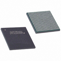
EP3C25F324I7 Altera, EP3C25F324I7 Datasheet - Page 174

EP3C25F324I7
Manufacturer Part Number
EP3C25F324I7
Description
IC CYCLONE III FPGA 25K 324 FBGA
Manufacturer
Altera
Series
Cyclone® IIIr
Datasheets
1.EP3C5F256C8N.pdf
(5 pages)
2.EP3C5F256C8N.pdf
(34 pages)
3.EP3C5F256C8N.pdf
(66 pages)
4.EP3C5F256C8N.pdf
(14 pages)
5.EP3C5F256C8N.pdf
(76 pages)
6.EP3C25F324I7.pdf
(274 pages)
Specifications of EP3C25F324I7
Number Of Logic Elements/cells
24624
Number Of Labs/clbs
1539
Total Ram Bits
608256
Number Of I /o
215
Voltage - Supply
1.15 V ~ 1.25 V
Mounting Type
Surface Mount
Operating Temperature
-40°C ~ 100°C
Package / Case
324-FBGA
Family Name
Cyclone III
Number Of Logic Blocks/elements
24624
# I/os (max)
215
Frequency (max)
437.5MHz
Process Technology
65nm
Operating Supply Voltage (typ)
1.2V
Logic Cells
24624
Ram Bits
608256
Operating Supply Voltage (min)
1.15V
Operating Supply Voltage (max)
1.25V
Operating Temp Range
-40C to 100C
Operating Temperature Classification
Industrial
Mounting
Surface Mount
Pin Count
324
Package Type
FBGA
For Use With
544-2370 - KIT STARTER CYCLONE III EP3C25
Lead Free Status / RoHS Status
Contains lead / RoHS non-compliant
Number Of Gates
-
Lead Free Status / Rohs Status
Not Compliant
Available stocks
Company
Part Number
Manufacturer
Quantity
Price
Company:
Part Number:
EP3C25F324I7N
Manufacturer:
ALTERA32
Quantity:
181
9–14
Cyclone III Device Handbook, Volume 1
In the AS configuration scheme, the serial configuration device latches input and
control signals on the rising edge of DCLK and drives out configuration data on the
falling edge. Cyclone III device family drives out control signals on the falling edge of
DCLK and latch configuration data on the falling edge of DCLK.
In configuration mode, the Cyclone III device family enables the serial configuration
device by driving the nCSO output pin low, which connects to the nCS pin of the
configuration device. The Cyclone III device family uses the DCLK and DATA[1]pins
to send operation commands and read address signals to the serial configuration
device. The configuration device provides data on its DATA pin, which connects to the
DATA[0] input of the Cyclone III device family.
After all the configuration bits are received by the Cyclone III device family, it releases
the open-drain CONF_DONE pin, which is pulled high by an external 10-kΩ resistor.
Initialization begins only after the CONF_DONE signal reaches a logic-high level. All
AS configuration pins (DATA[0], DCLK, nCSO, and DATA[1]) have weak internal
pull-up resistors that are always active. After configuration, these pins are set as input
tri-stated and are driven high by weak internal pull-up resistors. The CONF_DONE pin
must have an external 10-kΩ pull-up resistor for the device to initialize.
The timing parameters for AS mode are not listed here because the t
t
mode listed in
Multi-Device AS Configuration
You can configure multiple Cyclone III device family using a single serial
configuration device. You can cascade multiple Cyclone III device family using the
chip-enable (nCE) and chip-enable-out (nCEO) pins. The first device in the chain must
have its nCE pin connected to GND. You must connect its nCEO pin to the nCE pin of
the next device in the chain. Use an external 10-kΩ pull-up resistor to pull the nCEO
signal high to its V
device captures all its configuration data from the bitstream, it drives the nCEO pin
low, enabling the next device in the chain. You can leave the nCEO pin of the last
device unconnected or use it as a user I/O pin after configuration if the last device in
the chain is a Cyclone III device family. The nCONFIG, nSTATUS, CONF_DONE, DCLK,
and DATA[0] pins of each device in the chain are connected
STATUS
, t
CF2ST1
Chapter 9: Configuration, Design Security, and Remote System Upgrades in the Cyclone III Device Family
, and t
Table 9–13 on page
CD2UM
CCIO
level to help the internal weak pull-up resistor. When the first
timing parameters are identical to the timing parameters for PS
9–39.
© December 2009 Altera Corporation
(Figure
CF2CD
9–4).
Configuration Features
, t
CF2ST0
, t
CFG
,


