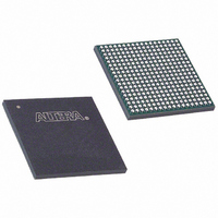
EP3C25F324I7 Altera, EP3C25F324I7 Datasheet - Page 107

EP3C25F324I7
Manufacturer Part Number
EP3C25F324I7
Description
IC CYCLONE III FPGA 25K 324 FBGA
Manufacturer
Altera
Series
Cyclone® IIIr
Datasheets
1.EP3C5F256C8N.pdf
(5 pages)
2.EP3C5F256C8N.pdf
(34 pages)
3.EP3C5F256C8N.pdf
(66 pages)
4.EP3C5F256C8N.pdf
(14 pages)
5.EP3C5F256C8N.pdf
(76 pages)
6.EP3C25F324I7.pdf
(274 pages)
Specifications of EP3C25F324I7
Number Of Logic Elements/cells
24624
Number Of Labs/clbs
1539
Total Ram Bits
608256
Number Of I /o
215
Voltage - Supply
1.15 V ~ 1.25 V
Mounting Type
Surface Mount
Operating Temperature
-40°C ~ 100°C
Package / Case
324-FBGA
Family Name
Cyclone III
Number Of Logic Blocks/elements
24624
# I/os (max)
215
Frequency (max)
437.5MHz
Process Technology
65nm
Operating Supply Voltage (typ)
1.2V
Logic Cells
24624
Ram Bits
608256
Operating Supply Voltage (min)
1.15V
Operating Supply Voltage (max)
1.25V
Operating Temp Range
-40C to 100C
Operating Temperature Classification
Industrial
Mounting
Surface Mount
Pin Count
324
Package Type
FBGA
For Use With
544-2370 - KIT STARTER CYCLONE III EP3C25
Lead Free Status / RoHS Status
Contains lead / RoHS non-compliant
Number Of Gates
-
Lead Free Status / Rohs Status
Not Compliant
Available stocks
Company
Part Number
Manufacturer
Quantity
Price
Company:
Part Number:
EP3C25F324I7N
Manufacturer:
ALTERA32
Quantity:
181
Chapter 6: I/O Features in the Cyclone III Device Family
OCT Support
LVDS Transmitter Programmable Pre-Emphasis
OCT Support
Table 6–3. Selectable I/O Drivers for On-Chip Series Termination with and Without Calibration Setting (Part 1 of 2)
© December 2009
3.0-V LVTTL/LVCMOS
2.5-V LVTTL/LVCMOS
1.8-V LVTTL/LVCMOS
1.5-V LVCMOS
1.2-V LVCMOS
SSTL-2 Class I
SSTL-2 Class II
I/O Standard
f
1
Altera Corporation
The Cyclone III device family true LVDS transmitter supports programmable
pre-emphasis. Programmable pre-emphasis is used to compensate the
frequency-dependent attenuation of the transmission line. It increases the amplitude
of the high-frequency components of the output signal, which cancels out much of the
high-frequency loss of the transmission line.
The Quartus II software allows two settings for programmable pre-emphasis
control—0 and 1, in which 0 is pre-emphasis off and 1 is pre-emphasis on. The default
setting is 1. The amount of pre-emphasis needed depends on the amplification of the
high-frequency components along the transmission line. You must adjust the setting
to suit your designs, as pre-emphasis decreases the amplitude of the low-frequency
component of the output signal as well.
For more information about the Cyclone III device family high-speed differential
interface support, refer to the
chapter.
The Cyclone III device family features OCT to provide I/O impedance matching and
termination capabilities. OCT helps to prevent reflections and maintain signal
integrity while minimizing the need for external resistors in high pin-count ball grid
array (BGA) packages. The Cyclone III device family provides I/O driver on-chip
impedance matching and on-chip series termination for single-ended outputs and
bidirectional pins.
When using on-chip series termination, programmable current strength is not
available.
There are two ways to implement OCT in the Cyclone III device family:
■
■
Table 6–3
termination.
On-Chip Series Termination with Calibration
OCT with calibration
OCT without calibration
Row I/O
50, 25
50, 25
50, 25
50, 25
lists the I/O standards that support impedance matching and series
50
50
25
Setting, in ohms (Ω)
Column I/O
50, 25
50, 25
50, 25
50, 25
50, 25
High-Speed Differential Interfaces in Cyclone III Devices
50
25
On-Chip Series Termination Without Calibration
Row I/O
50, 25
50, 25
50, 25
50, 25
50
50
25
Setting, in ohms (Ω)
Cyclone III Device Handbook, Volume 1
Column I/O
50, 25
50, 25
50, 25
50, 25
50, 25
50
25
6–7


