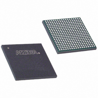
EP3C25F324I7 Altera, EP3C25F324I7 Datasheet - Page 203

EP3C25F324I7
Manufacturer Part Number
EP3C25F324I7
Description
IC CYCLONE III FPGA 25K 324 FBGA
Manufacturer
Altera
Series
Cyclone® IIIr
Datasheets
1.EP3C5F256C8N.pdf
(5 pages)
2.EP3C5F256C8N.pdf
(34 pages)
3.EP3C5F256C8N.pdf
(66 pages)
4.EP3C5F256C8N.pdf
(14 pages)
5.EP3C5F256C8N.pdf
(76 pages)
6.EP3C25F324I7.pdf
(274 pages)
Specifications of EP3C25F324I7
Number Of Logic Elements/cells
24624
Number Of Labs/clbs
1539
Total Ram Bits
608256
Number Of I /o
215
Voltage - Supply
1.15 V ~ 1.25 V
Mounting Type
Surface Mount
Operating Temperature
-40°C ~ 100°C
Package / Case
324-FBGA
Family Name
Cyclone III
Number Of Logic Blocks/elements
24624
# I/os (max)
215
Frequency (max)
437.5MHz
Process Technology
65nm
Operating Supply Voltage (typ)
1.2V
Logic Cells
24624
Ram Bits
608256
Operating Supply Voltage (min)
1.15V
Operating Supply Voltage (max)
1.25V
Operating Temp Range
-40C to 100C
Operating Temperature Classification
Industrial
Mounting
Surface Mount
Pin Count
324
Package Type
FBGA
For Use With
544-2370 - KIT STARTER CYCLONE III EP3C25
Lead Free Status / RoHS Status
Contains lead / RoHS non-compliant
Number Of Gates
-
Lead Free Status / Rohs Status
Not Compliant
Available stocks
Company
Part Number
Manufacturer
Quantity
Price
Company:
Part Number:
EP3C25F324I7N
Manufacturer:
ALTERA32
Quantity:
181
Chapter 9: Configuration, Design Security, and Remote System Upgrades in the Cyclone III Device Family
Configuration Features
FPP Configuration
© December 2009
f
1
1
Altera Corporation
The FPP configuration in Cyclone III device family is designed to meet the increasing
demand for faster configuration time. Cyclone III device family is designed with the
capability of receiving byte-wide configuration data per clock cycle.
You can perform the FPP configuration of Cyclone III device family with an intelligent
host, such as a MAX II device or microprocessor with flash memory. If your system
already contains a CFI flash memory, you can use it for the Cyclone III device family
configuration storage as well. The MAX II PFL feature in MAX II devices provides an
efficient method to program CFI flash memory devices through the JTAG interface
and the logic to control configuration from the flash memory device to the Cyclone III
device family. Both PS and FPP configuration schemes are supported using this PFL
feature.
For more information about the PFL, refer to
with the Quartus II
Cyclone III device family does not support enhanced configuration devices for PS or
FPP configurations.
FPP configuration is not supported in the E144 package of Cyclone III devices.
FPP Configuration Using an External Host
The FPP configuration using an external host provides a fast method to configure
Cyclone III device family. In the FPP configuration scheme, you can use an external
host device to control the transfer of configuration data from a storage device, such as
flash memory, to the target Cyclone III device family. You can store configuration data
in either an .rbf, .hex, or .ttf format. When using the external host, a design that
controls the configuration process, such as fetching the data from flash memory and
sending it to the device, must be stored in the external host device.
the configuration interface connections between the Cyclone III device family and an
external device for single-device configuration.
Figure 9–20. Single-Device FPP Configuration Using an External Host
Notes to
(1) Connect the pull-up resistor to a supply that provides an acceptable input signal for the device. V
(2) The nCEO pin is left unconnected or used as a user I/O pin when it does not feed the nCE pin of another device.
(3) The MSEL pin settings vary for different configuration voltage standards and POR time. To connect MSEL[3..0],
(4) All I/O inputs must maintain a maximum AC voltage of 4.1 V. DATA[7..0] and DCLK must fit the maximum
enough to meet the V
refer to
overshoot equation outlined in
Figure
Table 9–7 on page
9–20:
(MAX II Device or
Microprocessor)
External Host
Software.
IH
specification of the I/O on the device and the external host.
ADDR
9–11. Connect the MSEL pins directly to V
Memory
“Configuration and JTAG Pin I/O Requirements” on page
DATA[7..0]
10 k
V CCIO (1) V CCIO (1)
10 k
GND
AN 386: Using the Parallel Flash Loader
Cyclone III Device Family
CONF_DONE
nSTATUS
nCE
DATA[7..0] (4)
nCONFIG
DCLK (4)
CCA
or GND.
MSEL[3..0]
Cyclone III Device Handbook, Volume 1
nCEO
N.C. (2)
9–7.
Figure 9–20
(3)
CC
must be high
shows
9–43


