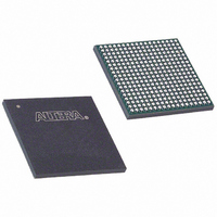
EP3C25F324I7 Altera, EP3C25F324I7 Datasheet - Page 142

EP3C25F324I7
Manufacturer Part Number
EP3C25F324I7
Description
IC CYCLONE III FPGA 25K 324 FBGA
Manufacturer
Altera
Series
Cyclone® IIIr
Datasheets
1.EP3C5F256C8N.pdf
(5 pages)
2.EP3C5F256C8N.pdf
(34 pages)
3.EP3C5F256C8N.pdf
(66 pages)
4.EP3C5F256C8N.pdf
(14 pages)
5.EP3C5F256C8N.pdf
(76 pages)
6.EP3C25F324I7.pdf
(274 pages)
Specifications of EP3C25F324I7
Number Of Logic Elements/cells
24624
Number Of Labs/clbs
1539
Total Ram Bits
608256
Number Of I /o
215
Voltage - Supply
1.15 V ~ 1.25 V
Mounting Type
Surface Mount
Operating Temperature
-40°C ~ 100°C
Package / Case
324-FBGA
Family Name
Cyclone III
Number Of Logic Blocks/elements
24624
# I/os (max)
215
Frequency (max)
437.5MHz
Process Technology
65nm
Operating Supply Voltage (typ)
1.2V
Logic Cells
24624
Ram Bits
608256
Operating Supply Voltage (min)
1.15V
Operating Supply Voltage (max)
1.25V
Operating Temp Range
-40C to 100C
Operating Temperature Classification
Industrial
Mounting
Surface Mount
Pin Count
324
Package Type
FBGA
For Use With
544-2370 - KIT STARTER CYCLONE III EP3C25
Lead Free Status / RoHS Status
Contains lead / RoHS non-compliant
Number Of Gates
-
Lead Free Status / Rohs Status
Not Compliant
Available stocks
Company
Part Number
Manufacturer
Quantity
Price
Company:
Part Number:
EP3C25F324I7N
Manufacturer:
ALTERA32
Quantity:
181
7–18
Software Overview
Cyclone III Device Handbook, Volume 1
f
f
1
■
■
■
■
■
■
■
■
■
■
For more information about PCB layout guidelines, refer to
Layout Guidelines
Cyclone III device family high-speed I/O system interfaces are created in core logic
by a Quartus II software megafunction because they do not have a dedicated circuit
for the SERDES. The Cyclone III device family uses the I/O registers and LE registers
to improve the timing performance and support the SERDES. Altera Quartus II
software allows you to design your high-speed interfaces using the ALTLVDS
megafunction. This megafunction implements either a high-speed deserializer
receiver or a high-speed serializer transmitter. There is a list of parameters in the
ALTLVDS megafunction that you can set to customize your SERDES based on your
design requirements. The megafunction is optimized to use Cyclone III device family
resources to create high-speed I/O interfaces in the most effective manner.
When you are using the Cyclone III device family with the ALTLVDS megafunction,
the interface always sends the MSB of your parallel data first.
For more information about designing your high-speed I/O systems interfaces using
the ALTLVDS megafunction, refer to the
Quartus II
Use surface mount components.
Avoid 90° corners on board traces.
Use high-performance connectors.
Design backplane and card traces so that trace impedance matches the impedance
of the connector and termination.
Keep an equal number of vias for both signal traces.
Create equal trace lengths to avoid skew between signals. Unequal trace lengths
result in misplaced crossing points and decrease system margins as the
transmitter-channel-to-channel skew (TCCS) value increases.
Limit vias because they cause discontinuities.
Keep switching transistor-to-transistor logic (TTL) signals away from differential
signals to avoid possible noise coupling.
Do not route TTL clock signals to areas under or above the differential signals.
Analyze system-level signals.
Handbook.
and
AN 315: Guidelines for Designing High-Speed FPGA
Chapter 7: High-Speed Differential Interfaces in the Cyclone III Device Family
ALTLVDS Megafunction User Guide
© December 2009 Altera Corporation
AN 224: High-Speed Board
PCBs.
Software Overview
and the


