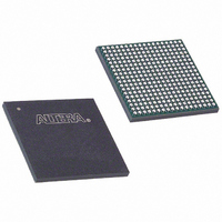
EP3C25F324I7 Altera, EP3C25F324I7 Datasheet - Page 139

EP3C25F324I7
Manufacturer Part Number
EP3C25F324I7
Description
IC CYCLONE III FPGA 25K 324 FBGA
Manufacturer
Altera
Series
Cyclone® IIIr
Datasheets
1.EP3C5F256C8N.pdf
(5 pages)
2.EP3C5F256C8N.pdf
(34 pages)
3.EP3C5F256C8N.pdf
(66 pages)
4.EP3C5F256C8N.pdf
(14 pages)
5.EP3C5F256C8N.pdf
(76 pages)
6.EP3C25F324I7.pdf
(274 pages)
Specifications of EP3C25F324I7
Number Of Logic Elements/cells
24624
Number Of Labs/clbs
1539
Total Ram Bits
608256
Number Of I /o
215
Voltage - Supply
1.15 V ~ 1.25 V
Mounting Type
Surface Mount
Operating Temperature
-40°C ~ 100°C
Package / Case
324-FBGA
Family Name
Cyclone III
Number Of Logic Blocks/elements
24624
# I/os (max)
215
Frequency (max)
437.5MHz
Process Technology
65nm
Operating Supply Voltage (typ)
1.2V
Logic Cells
24624
Ram Bits
608256
Operating Supply Voltage (min)
1.15V
Operating Supply Voltage (max)
1.25V
Operating Temp Range
-40C to 100C
Operating Temperature Classification
Industrial
Mounting
Surface Mount
Pin Count
324
Package Type
FBGA
For Use With
544-2370 - KIT STARTER CYCLONE III EP3C25
Lead Free Status / RoHS Status
Contains lead / RoHS non-compliant
Number Of Gates
-
Lead Free Status / Rohs Status
Not Compliant
Available stocks
Company
Part Number
Manufacturer
Quantity
Price
Company:
Part Number:
EP3C25F324I7N
Manufacturer:
ALTERA32
Quantity:
181
Chapter 7: High-Speed Differential Interfaces in the Cyclone III Device Family
True Output Buffer Feature
Figure 7–13. Differential HSTL Class II Interface
Note to
(1) PLL output clock pins do not support differential HSTL Class II I/O standard.
True Output Buffer Feature
Programmable Pre-Emphasis
Figure 7–14. The Output Signal with Pre-Emphasis
© December 2009
Figure
Output Buffer (1)
7–13:
Altera Corporation
Figure 7–13
Cyclone III device family true differential transmitters offer programmable
pre-emphasis—you can choose to turn it on or off. The default setting is on.
The programmable pre-emphasis boosts the high frequencies of the output signal to
compensate the frequency-dependant attenuation of the transmission line to
maximize the data eye opening at the far-end receiver. Without pre-emphasis, the
output current is limited by the V
transmitter. At high frequency, the slew rate may not be fast enough to reach full V
before the next edge; this may lead to pattern dependent jitter. With pre-emphasis, the
output current is momentarily boosted during switching to increase the output slew
rate. The overshoot produced by this extra switching current is different from the
overshoot caused by signal reflection. This overshoot happens only during switching,
and does not produce ringing.
Figure 7–14
shows the differential HSTL Class II interface.
shows the differential output signal with pre-emphasis.
Negative channel (n)
V
Positive channel (p)
TT
50 Ω
V
TT
50 Ω
Z 0 = 50 Ω
Z 0 = 50 Ω
OD
specification and the output impedance of the
V
TT
Overshoot
Undershoot
V
50 Ω
OD
V
TT
50 Ω
Cyclone III Device Handbook, Volume 1
Receiver
7–15
OD


