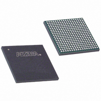
EP3C25F324I7 Altera, EP3C25F324I7 Datasheet - Page 136

EP3C25F324I7
Manufacturer Part Number
EP3C25F324I7
Description
IC CYCLONE III FPGA 25K 324 FBGA
Manufacturer
Altera
Series
Cyclone® IIIr
Datasheets
1.EP3C5F256C8N.pdf
(5 pages)
2.EP3C5F256C8N.pdf
(34 pages)
3.EP3C5F256C8N.pdf
(66 pages)
4.EP3C5F256C8N.pdf
(14 pages)
5.EP3C5F256C8N.pdf
(76 pages)
6.EP3C25F324I7.pdf
(274 pages)
Specifications of EP3C25F324I7
Number Of Logic Elements/cells
24624
Number Of Labs/clbs
1539
Total Ram Bits
608256
Number Of I /o
215
Voltage - Supply
1.15 V ~ 1.25 V
Mounting Type
Surface Mount
Operating Temperature
-40°C ~ 100°C
Package / Case
324-FBGA
Family Name
Cyclone III
Number Of Logic Blocks/elements
24624
# I/os (max)
215
Frequency (max)
437.5MHz
Process Technology
65nm
Operating Supply Voltage (typ)
1.2V
Logic Cells
24624
Ram Bits
608256
Operating Supply Voltage (min)
1.15V
Operating Supply Voltage (max)
1.25V
Operating Temp Range
-40C to 100C
Operating Temperature Classification
Industrial
Mounting
Surface Mount
Pin Count
324
Package Type
FBGA
For Use With
544-2370 - KIT STARTER CYCLONE III EP3C25
Lead Free Status / RoHS Status
Contains lead / RoHS non-compliant
Number Of Gates
-
Lead Free Status / Rohs Status
Not Compliant
Available stocks
Company
Part Number
Manufacturer
Quantity
Price
Company:
Part Number:
EP3C25F324I7N
Manufacturer:
ALTERA32
Quantity:
181
7–12
Figure 7–7. RSDS Interface with Single Resistor Network on the Top and Bottom I/O Banks
Note to
(1)
LVPECL I/O Support in the Cyclone III Device Family
Figure 7–8. LVPECL AC-Coupled Termination
Cyclone III Device Handbook, Volume 1
R
P
Figure
= 100
Ω
7–7:
f
Cyclone III Device Family
RSDS Transmitter
Figure 7–7
bottom I/O banks.
The LVPECL I/O standard is a differential interface standard that requires a 2.5-V
V
telecommunications, data communications, and clock distribution. The Cyclone III
device family supports the LVPECL input standard at the dedicated clock input pins
only. The LVPECL receiver requires an external 100-Ω termination resistor between
the two signals at the input buffer.
For more information about the LVPECL I/O standard electrical specification, refer to
the
AC coupling is required when the LVPECL common mode voltage of the output
buffer is higher than the Cyclone III device family LVPECL input common mode
voltage.
Figure 7–8
receiver are external to the device. DC-coupled LVPECL is supported if the LVPECL
output common mode voltage is in the Cyclone III device family LVPECL input buffer
specification
CCIO.
Emulated
Cyclone III Device Data Sheet
Transmitter
LVPECL
This standard is used in applications involving video graphics,
shows the RSDS interface with a single resistor network on the top and
shows the AC-coupled termination scheme. The 50-Ω resistors used at the
(Figure
Single Resistor Network
0.1 µF
0.1 µF
7–9).
R
P
Chapter 7: High-Speed Differential Interfaces in the Cyclone III Device Family
Z 0 = 50
Z 0 = 50
and
Cyclone III LS Device Data Sheet
V ICM
50 Ω
50 Ω
50
50
100 Ω
Cyclone III Device Family
LVPECL Receiver
RSDS Receiver
© December 2009 Altera Corporation
High-Speed I/O Standards Support
chapters.


