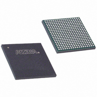
EP3C25F324I7 Altera, EP3C25F324I7 Datasheet - Page 113

EP3C25F324I7
Manufacturer Part Number
EP3C25F324I7
Description
IC CYCLONE III FPGA 25K 324 FBGA
Manufacturer
Altera
Series
Cyclone® IIIr
Datasheets
1.EP3C5F256C8N.pdf
(5 pages)
2.EP3C5F256C8N.pdf
(34 pages)
3.EP3C5F256C8N.pdf
(66 pages)
4.EP3C5F256C8N.pdf
(14 pages)
5.EP3C5F256C8N.pdf
(76 pages)
6.EP3C25F324I7.pdf
(274 pages)
Specifications of EP3C25F324I7
Number Of Logic Elements/cells
24624
Number Of Labs/clbs
1539
Total Ram Bits
608256
Number Of I /o
215
Voltage - Supply
1.15 V ~ 1.25 V
Mounting Type
Surface Mount
Operating Temperature
-40°C ~ 100°C
Package / Case
324-FBGA
Family Name
Cyclone III
Number Of Logic Blocks/elements
24624
# I/os (max)
215
Frequency (max)
437.5MHz
Process Technology
65nm
Operating Supply Voltage (typ)
1.2V
Logic Cells
24624
Ram Bits
608256
Operating Supply Voltage (min)
1.15V
Operating Supply Voltage (max)
1.25V
Operating Temp Range
-40C to 100C
Operating Temperature Classification
Industrial
Mounting
Surface Mount
Pin Count
324
Package Type
FBGA
For Use With
544-2370 - KIT STARTER CYCLONE III EP3C25
Lead Free Status / RoHS Status
Contains lead / RoHS non-compliant
Number Of Gates
-
Lead Free Status / Rohs Status
Not Compliant
Available stocks
Company
Part Number
Manufacturer
Quantity
Price
Company:
Part Number:
EP3C25F324I7N
Manufacturer:
ALTERA32
Quantity:
181
Chapter 6: I/O Features in the Cyclone III Device Family
Termination Scheme for I/O Standards
Table 6–4. Cyclone III Device Family Supported I/O Standards and Constraints (Part 2 of 2)
Termination Scheme for I/O Standards
Voltage-Referenced I/O Standard Termination
© December 2009
RSDS and
mini-LVDS
BLVDS
LVPECL
Notes to
(1) The PCI-clamp diode must be enabled for 3.3-V/3.0-V LVTTL/LVCMOS.
(2) Differential HSTL and SSTL outputs use two single-ended outputs with the second output programmed as inverted. Differential HSTL and SSTL
(3) PPDS, mini-LVDS, and RSDS are only supported on output pins.
(4) LVPECL is only supported on clock inputs.
(5) Bus LVDS (BLVDS) output uses two single-ended outputs with the second output programmed as inverted. BLVDS input uses LVDS input buffer.
(6) Class I and Class II refer to output termination and do not apply to input. 1.2-V HSTL input is supported at both column and row I/O regardless of
(7) True differential LVDS, RSDS, and mini-LVDS I/O standards are supported in left and right I/O pins while emulated differential LVDS, RSDS, and
I/O Standard
inputs treat differential inputs as two single-ended HSTL and SSTL inputs and only decode one of them. Differential HSTL and SSTL are only
supported on CLK pins.
class.
mini-LVDS I/O standards are supported in both left and right, and top and bottom I/O pins.
(5)
Table
(4)
(3)
6–4:
Altera Corporation
Differential
Differential
Differential
The Cyclone III device family supports PCI and PCI-X I/O standards at 3.0-V V
The 3.0-V PCI and PCI-X I/O are fully compatible for direct interfacing with 3.3-V PCI
systems without requiring any additional components. The 3.0-V PCI and PCI-X
outputs meet the V
sufficient noise margin.
This section describes recommended termination schemes for voltage-referenced and
differential I/O standards.
The 3.3-V LVTTL, 3.0-V LVTTL and LVCMOS, 2.5-V LVTTL and LVCMOS, 1.8-V
LVTTL and LVCMOS, 1.5-V LVCMOS, 1.2-V LVCMOS, 3.0-V PCI, and PCI-X
I/O standards do not specify a recommended termination scheme per the JEDEC
standard
Voltage-referenced I/O standards require an input reference voltage (V
termination voltage (V
termination voltage of the transmitting device, as shown in
Type
Standard
Support
—
—
—
IH
and V
TT
). The reference voltage of the receiving device tracks the
IL
Input
requirements of 3.3-V PCI and PCI-X inputs with
2.5
2.5
V
—
C CIO
Level (in V)
Output
2.5
2.5
—
CLK,
DQS
Top and Bottom I/O Pins
—
—
v
PLL_OUT
Cyclone III Device Handbook, Volume 1
v
—
—
Figure 6–6
User
Pins
I/O
v
v
—
and
REF
) and a
Figure
CLK,
Left and Right
DQS
v
—
—
I/O Pins
CCIO
User I/O
6–7.
6–13
.
Pins
v
v
—


